Introduction
If some basic layout guidelines are not followed, the PCB design will limit the performance or reduce the reliability of the Class D amplifier. The following describes some of the good PC board layout practices for Class D amplifiers. The STA517B (175 watts per channel) digital power amplifier with two BTL outputs is used as an example, but the basic concept is the same for all Class D amplifiers.

Figure 1: Schematic diagram of a stereo BTL Class D power amplifier
horizon
A good ground plane is the key to a high quality Class D amplifier layout. If possible, the bottom layer of the board should be a proprietary ground plane, and the full ground plane provides the best performance and the most reliable design. If you have to route signal lines or power traces on the bottom of the board, be as short as possible. If necessary, in order to make the underlying traces short distances, the traces should be routed back to the top layer of the board to avoid long-distance traces at the bottom.
Use vias to connect the top device of the board to the ground plane of the underlying board. However, vias still block current flow back to ground level, so these vias must be used flexibly.
The area directly under the amplifier must be copper. If the amplifier has an exposed pad or plug-in at the bottom of its package, the IC must be soldered to the ground where the amplifier is placed, which can be used as the fan's hot zone. In this case, the ground must be drawn from both sides of the IC in the down direction to ensure that it is bare. The ground below the amplifier must be filled with a number of vias that fan through the vias to the bottom of the board, so it can also act as a fan area.
Just below the amplifier is not recommended to go the signal line. Several vias must be connected to the ground plane to ensure that all devices have a direct and low impedance path to the ground reference point. This is especially important for output filters. All filter grounds must have a direct path back to the ground plane directly below the amplifier.
Power supply bypass capacitor
To ensure stability and to suppress noise and crosstalk, it is very important to add bypass capacitors to the power supply. The output stage of the amplifier draws a large amount of current and the switching action is fast. When the output switch is activated, the parasitic inductance between the bypass capacitor and the amplifier power input pin generates a large glitch, so the parasitic inductance must be kept as small as possible. In order to reduce the effects of resonance between the stray inductance and the bypass capacitor at the amplifier power stage, a 100nF capacitor should be used in parallel with the 1uF capacitor at each power input pin.
The 100nF capacitor must be as close as possible to the IC (usually no more than 2mm). Moreover, as shown in Figure 1, the bypass capacitor must be on the same layer as the IC to reduce the total path length (and stray inductance). The 1uF capacitors must be placed in turn, close to the 100nF capacitor.

Figure 2: Using the bottom layer of the board to ground the 100nF capacitor, this will significantly increase the total trace length and adversely affect board performance.
It is also necessary to use a large-capacity storage capacitor to decouple the amplifier's power input. The capacitance of a large volume storage capacitor depends on the amount of current required by the amplifier. The bulk storage capacitor must be star-connected to the amplifier and power pin and must be as close as possible to the amplifier (ideally less than 30 mm).
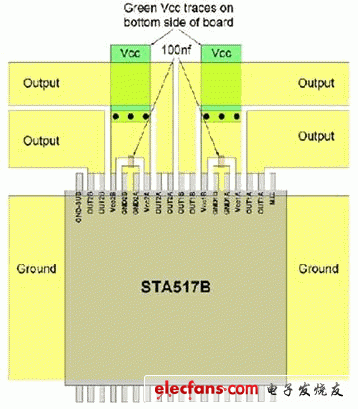
Figure 3: The 100nF bypass capacitor must be placed close to the IC.
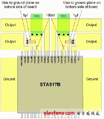
Figure 4: The 1uF capacitor needs to be placed after the 100nF capacitor, and the 1uF capacitor is connected to the ground plane of the bottom layer of the board through the via.
iPhone X 3D viewer is a protective iPhone X case,but also a 3D Viewer For Iphone X, It is a bare-eye VR viewer in phone case shape. When the users cover it on smartphone screen, he can enjoy 3D videos and games without wearing 3D glasses or VR headset. MOPIC Mplayer3D Application should be used together with the Snap3D, to search for 3D videos, 3D images, 3D games from Youtube, or search within the resources which are connected to Maplayer3D. It's light weight, easy to carry as well.
HOW TO USE THE SNAP3D AS A 3D SCREEN
The attached 3D screen on the Snap3D acts
like 3D glasses.
To turn your smartphone into a 3D device, you need to first download the
[Mplayer3D" application.
Then install the Snap3D on your smartphone screen and run Mplayer3D.
Enjoy the stunning stereoscopic 3D!


Iphone X 3D Viewer,Iphone X Vr Viewer,3D Viewer For Iphone X,Vr Viewer For Iphone X
iSID Korea Co., Ltd , https://www.isidsnap3d.com