The lithography machine is hailed as one of the 20th century invention miracles of mankind. We use the mobile phone's CPU manufacturing process can not be separated from the lithography machine.
The lithography machine is an enlarged SLR. The lithography machine prints the designed integrated circuit pattern on the mask onto the photosensitive material through the exposure of light to form a pattern. The core is the lens. This is not an ordinary lens. It can reach a height of 2 meters, a diameter of 1 meter, and even more. At present, there are five companies with ASML in the Netherlands, Nikon in Japan, cannon in Japan, ultratech in the United States, and SMEE in China. The lithography machine is hailed as the jewel in the crown of the integrated circuit industry by the industry, and the technical threshold and funding threshold for R&D are very high.
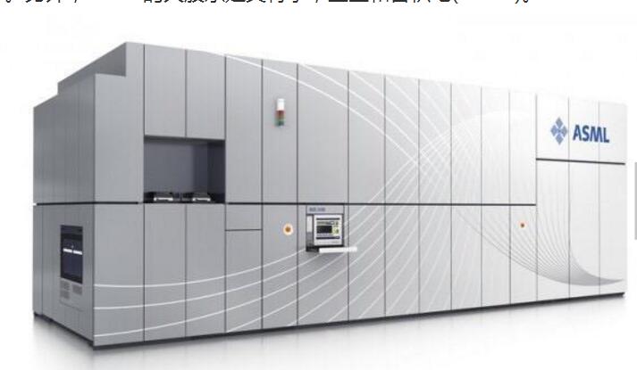
1. Dutch lithography giant ASML:
ASML (full name: Advanced Semiconductor Material Lithography, ASML Holding NV), Chinese name as Asma (China), Esmol (Taiwan, China). Is one of the world's largest semiconductor equipment manufacturers headquartered in Veldhoven, The Netherlands, providing leading comprehensive integrated key equipment to complex IC manufacturers worldwide. ASML's shares are listed in Amsterdam and New York respectively. In addition, ASML's major shareholders are Intel, Samsung and Taiwan Semiconductor Manufacturing (TSMC).
The high-end market for lithography machines is as big as ASML, and Nikon and Canon have already exited the high-end lithography machine market. ASML Lens Germany Carl Zeiss (Carl Zeiss), light source Cymer (acquired by ASML in October 2012). The latest is the ASML second-generation EUV (extreme-ultraviolet) lithography machine, which sells for over $100 million each, but it is banned from the mainland.
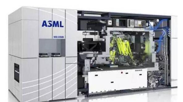
2. Japan's Nikon and Canon
As one of the only three companies in the world that can manufacture commercial lithography machines, Nikon seems to be not known to many people in this area. Many people only know that Nikon's cameras are doing well, but they do not know that Nikon lithography machines are equally renowned. global.
Lithography machine as the most critical equipment for the entire integrated circuit manufacturing, the performance of its equipment directly affects the development of the entire microelectronics industry. The world's most advanced immersion lithography machine is currently only produced by ASML, Nikon and Canon, and the price of a single unit is up to tens of millions of US dollars.
The Dutch ASML company has monopolized the high-end chip exposure machine market since 2011, has also controlled 80% of the low-end chip exposure market, and has 105% of the entire chip exposure market (because Nikon is losing money). This year, the monopoly pattern of ASML became more obvious. Canon recognized current affairs. In 2008, it gradually withdrew from the chip exposure business, stopped losing money and focused on the printer business. Mitsubishi, the largest consortium in Japan, was not willing to lose production capacity in this area and tried its best to support Nikon's chip exposure machine. The loss was not willing to withdraw, but the result was deeper and deeper.
Nikon's chip lithography machine is gradually declining. The Netherlands ASML takes a dominant position step by step. The only remaining advantage of Nikon lithography machines is that the price of similar models is less than half that of ASML. However, it was Intel that gave Nikon a fatal blow. In the new manufacturing process, it stopped purchasing Nikon's lithography machines. Only a few low-level and old-age lithography machines in all major semiconductor production lines that I know have been Nikon or Canon's. After all, now Intel, Samsung and TSMC have all become shareholders of ASML.
According to a report from Reuters, Nikon, the Japanese optical giant, said on the 24th that it has filed a lawsuit against ASML Holding NV, a Dutch semiconductor company, and its partner Carl Zeiss AG. It also stated that the two companies, ASML and Carl Zeiss, applied their lithography technology patents on lithography machines without the permission of Nikon, and applied them to the semiconductor manufacturing industry.
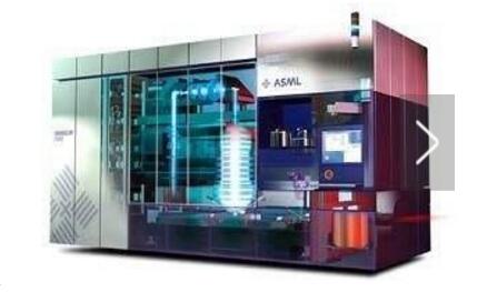
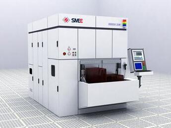
1, Shanghai Microelectronics Equipment Co., Ltd.
Shanghai Microelectronics Equipment Co., Ltd. has already mass-produced 90nm
2. The 45th Institute of China National Science and Technology Corporation
Neutron Science and Technology Corporation's 45th Institute Guodian has mass production of 1500 nm
3. Hefei Core Semiconductor Co., Ltd.
Hefei Core Semiconductor Co., Ltd. has produced the most advanced is 200 nanometers
4, first Teng Optoelectronics Technology Co., Ltd.
Teng Optoelectronics Technology Co., Ltd. has mass production of 800 nanometers
5. Wuxi Shadowspeed Semiconductor Technology Co., Ltd.
Wuxi Yingsha Semiconductor Technology Co., Ltd. 200nm
From the above data, it can be seen that the current leading technology is the development of the 65nm lithography machine of Shanghai Microelectronics Equipment Co., Ltd., a national major national science and technology major project “Very large scale integrated circuit manufacturing equipment and complete sets of process special projects†(02 special project). Conduct whole machine assessment. Specific technical analysis from 65 nm to 32 nm: The lithography technology is a technical step at 90 nm. It is easy to reach 45 nm after 90 nm, that is, you can make a 65 nm lithography machine, then for 65 nm The upgrade can do 45 nanometers. 45 nm is a technical step. With 45nm, it's easier to upgrade to 22nm. 22 nm is also a step. Stepping over 22nm, it is not difficult to upgrade to 14nm. China currently has 90 nanometers. It's not difficult to upgrade to 65nm with 90nm. But 45nm is a technological step. The 45nm R&D is much more difficult than 90nm and 65nm. If you solve the 45 nm that can be upgraded to 32 nm is not difficult. However, the next upgrade to 22 nm cannot be directly upgraded to 22 nm at 45 nm. 22nm uses many new technologies.
China's 02 special project of 16 major projects proposed that the lithography machine will produce 22 nanometers by 2020. In 2015, 45 nanometers and 65 nanometers were industrialized. Let's talk about 45 nanometers specifically. Because of the current mainstream lithography machine. Including 32 nanometers and 28 nanometers are basically upgraded and upgraded on the 45-nm invasive deep ultraviolet lithography machine. Therefore, it is very important for China to master 45 nanometers. At 65nm, the objective lens is upgraded to a diameter of 1.2 at 90nm. The 45 nm lithography machine is an important step. After reaching this level, the objective lens and polarized light upgrade on the 45 nm lithography machine can reach 32 nm.
In addition, solid-state deep-UV light sources for lithography machines are also under development. China's lithography machine R&D is being developed in parallel, and the technology used in the 22-nm lithography machine is also being researched and developed for use on the 45-nanometer upgrade. There are also electron beam direct-write lithography machines, nanoimprint equipment, and EUV lithography technology. Upgrading the photoresist, upgrading the refractive liquid, and using the engraved method can reach the level of 22 nm to 14 nm or even 10 nm. Correspondingly upgraded photoresists, 3rd generation refraction liquids, etc. are also being developed accordingly.
For a long time, China's lithography technology has lagged behind advanced countries and has become a shortcoming in China's industrial modernization process. Is there any major breakthrough in the development of the lithography machine?
The Acceptance Meeting for China's “Key Technology Research for Extreme Ultraviolet Lithography†project was held in Changchun Institute of Optics, Fine Mechanics and Physics, witnessed by many review experts on site, passed a series of results obtained by the project, and greatly advanced China’s extreme ultraviolet Development of lithography technology.
On November 15, 2016, the National Science and Technology Major Project 02 Special Project “Key Technology Research for Extreme Ultraviolet Lithography†led by Changchun Optical Engine Co., Ltd. was successfully tested before on-site testing. With the joint efforts of Changchun Institute of Optics, Chengdu Optoelectronics Institute, Shanghai Opto-Mechanics Institute, Institute of Microelectronics, Chinese Academy of Sciences, Beijing Institute of Technology, Harbin Institute of Technology, and Huazhong University of Science and Technology, after eight years of hard work, the company successfully Completed the pre-determined research contents and tasks, broke through the core optical technology that restricts the development of EUV lithography in China, and initially established a processing, inspection, coating, and system integration platform suitable for the development of EUV lithography exposure optical systems. It laid a solid foundation for the sustainable development of China's lithography technology.
Lithography is the core of the integrated circuit manufacturing industry and determines the feature size of integrated circuits. With the continuation of Moore's Law in the semiconductor industry, Extreme Ultraviolet Lithography (EUVL) is recognized as the most promising next-generation lithography technology.
EUV lithography is a type of projection lithography that uses 13.5nm EUV light as its operating wavelength. It is an extension of the conventional projection lithography technology to shorter wavelengths and is at the critical point of industrialization. As the integration of cutting-edge technologies in industrial manufacturing, only a few research institutions and companies in the world have mastered this technology. At present, the international monopoly of EUVL technology has already taken shape. It forms a technical blockade for China, and future sales policies are difficult to predict. China has been paying attention to and developing EUVL technology since the 1990s. Initially, it has carried out basic key technologies such as EUV light source, EUV multilayer film, and ultra-smooth polishing technology. In 2008, the National Science and Technology Major Project of “Very Large Scale Integrated Circuit Manufacturing Equipment and Complete Sets of Processes†listed the EUVL technology as a key issue for the next generation of lithography technology. “Made in China 2025†listed the EUVL as a development focus in the integrated circuit manufacturing field and planned In 2030, the localization of EUV lithography machines will be realized.
Under the traction of special task 02, the short-wave optical research team of Changguang Opto-Electronics Co., Ltd.'s light room should study hard and work hard. The EUV multi-layered film technology and deep sub-nanometers are used in the collaborative design of EUV optical systems and the film thickness control precision is atomic level. Advanced ultra-smooth aspheric surface processing and detection technology, ultra-high-precision objective lens system aberration detection and integration technology, etc., broke through a series of EUVL engineering key technology bottlenecks; successfully developed a small-field EUVL exposure optical system, projection objective wave The aberration is better than 0.75nm (RMS), and the EUVL static exposure device is constructed to obtain a 32nm line-width photoresist exposure pattern. The EUVL key technology verification and process test platform is established. Through the implementation of the project, we have successfully achieved the leap in the ultra-violet imaging optical technology and formed a research team with leading domestic and international advanced levels, which has laid a solid foundation for the engineering development of the EUV exposure optical system. technical foundation.
What is EUV lithography?
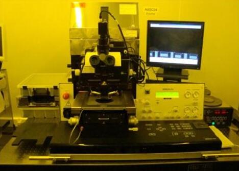
EUV lithography machine
Simply put, EUV lithography is a type of projection lithography that uses EUV light at a wavelength of 13.5 nm as the operating wavelength, which represents the highest level of current development in applied optics. As the next generation of lithography, the industry has been given the mission of saving Moore's Law.
CPU processor
The Changchun Institute of Optics and Mechanics of the Chinese Academy of Sciences has carried out relevant research in this field since the 1990s, but it is limited by foreign device technology blockades and its own technological weaknesses, and the progress has been far behind the rate of foreign development. In order to catch up with foreign technology in 2008, China has listed 32-22nm EUV lithography as an important research task. After nearly 8 years of hard work and research, China has finally succeeded and successfully broke the foreign technology blockade in this field.

smart phone
Lithography technology as an indispensable device for modern integrated circuit design, and the biggest bottleneck, is directly related to the development and progress of electronic chips such as CPUs. It is precisely because of the lag in China's EUV lithography technology that China has to import high-priced finished products from foreign countries. Recommended reading:
According to statistics, China has imported more than 1 trillion yuan worth of chips from the West for many years. This trend continues to rise. For example, last year exceeded 1,500 billion in a year. It can be said that IC has become the loss of public funds in China's treasury and The huge hole in national defense economic security.
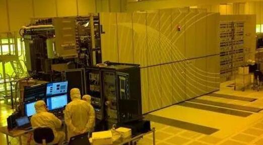
Experimental production chips
Therefore, the Changchun Optical Machine Co., Ltd. has made major breakthroughs in EUV lithography technology, its significance is no less than the electromagnetic ejection, and even comparable to the Emei engine.
gree , https://www.greegroups.com