The ever-increasing capacity of wireless networks and the growing demand for broadband multimedia components. Especially for dense local communications, the 60 GHz band assigned to the Wireless Personal Network (WPAN) has special significance for short-range communications. This is because the RF attenuation caused by atmospheric oxygen in the 8 GHz bandwidth centered at 60 GHz is 10 to 15 dB/km. This makes the 60 GHz band the most significant for all types of short-range wireless communications. In order to use the RF chip embedded system (SoC) method in a 60 GHz radio, an antenna incorporating a low-cost monolithic integrated CMOS RF front-end circuit was studied.
This paper presents a 60 GHz CMOS RF chip embedded dipole antenna. A planar dipole antenna structure with an integrated microstrip via unbalance-balancer is used in the design of such an RF chip embedded antenna. A FEM-based 3-D full-wave EM solver-Ansoft HFSS is used in the design simulation. The antenna chip is fabricated using a 0.18 micron CMOS process. The input VSWR of the designed RF chip embedded antenna and the antenna gain on the wafer are measured using a microwave probe station.
Antenna design
Figure 1 shows the proposed planar printed dipole antenna. Microstrip via imbalance - The balancer acts as an unbalanced-balanced converter between the feed coaxial line and the two printed dipole strips. The length of the dipole band is about 1/4 wavelength. The ground planes of the microstrip line and the dipole strip are on the same side. As indicated in the figure, the via allows the feed signal of one printed dipole (point 2) to have the same phase as the feed signal of the other printed dipole (point 1). Because there is a 180° difference between the top conductor and the ground plane of the microstrip line, there is a 180° difference between the feed signal of the printed dipole strip 2 and the other feed signal of point 1. The dipole armband width is chosen to be approximately one tenth of the wavelength. The characteristic impedance of the wide side of the microstrip feeder is designed to be 50 Ω. Printed Dipoles and Integrated Via Unbalance - The dimensions of each part of the balancer must be accurately numerically calculated to achieve the desired printed antenna performance. Figure 2 shows the chip layout and section view of the designed 0.1 GHz CMOS process of the 60 GHz RF chip embedded dipole antenna.
2. Simulation and test conclusions
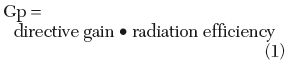
Figure 3 shows the antenna current distribution for the HFSS simulation. The simulated current density vector on the top and bottom metal clearly shows the equilibrium current distribution and the 180° phase difference of the current flow vector at the two printed dipole feed points. This demonstrates the role of the integrated microstrip imbalance-balancer. Figure 4 shows a micrograph of a chip fabricated into a 60 GHz CMOS RF chip embedded antenna. The chip size is 0.75 × 0.66mm and the substrate thickness is approximately 500mm. Figure 5 shows the measured values ​​on the antenna input VSWR wafer, which is less than 3 in 55 to 65 GHz. Figure 6 and Table 1 show the simulated radiation pattern of the 60 GHz antenna and the H-plane and E-plane power gain values. Note that the antenna power gain (absolute gain) Gp is ​​defined as:
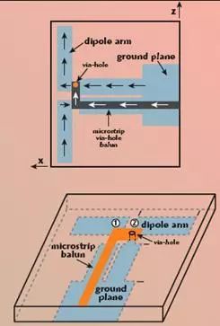
Figure 1 with integrated via imbalance
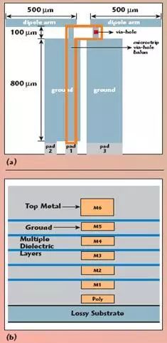
Figure 2 60GHz CMOS RF chip embedded antenna chip wiring (a) and cross-sectional view (b)
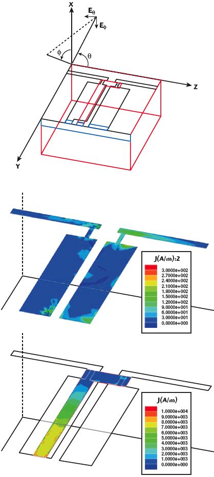
Figure 3 HFSS simulation and simulation antenna current distribution

Figure 4 chip micrograph
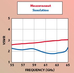
Figure 5 Simulation and measured antenna input VSWR
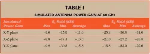
Table 1 60GHz simulated antenna power gain
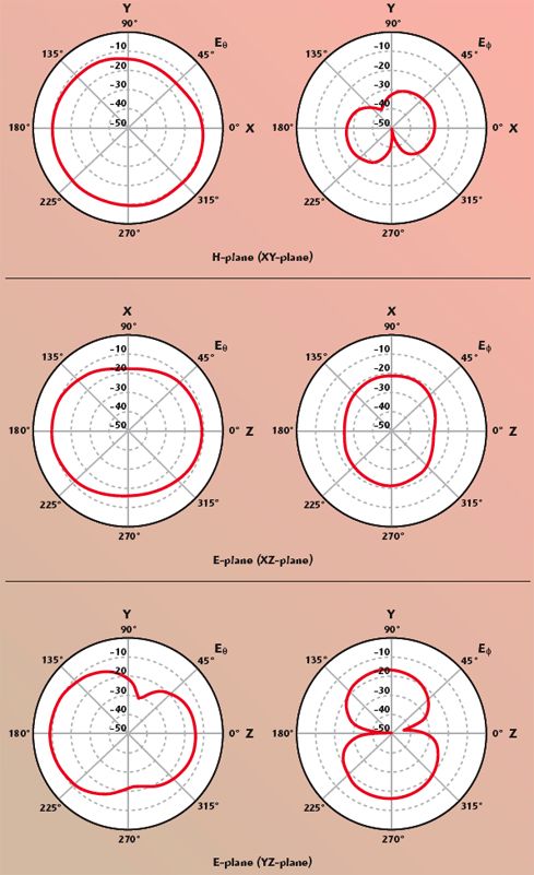
Figure 6 Radiation pattern of 60 GHz H-plane E-plane simulation antenna
The simulated antenna radiation efficiency is approximately 16 percent. This may be due to CMOS substrate losses. The H plan is approximately an omnidirectional pattern except that there is some attenuation in a particular direction. The H-plane simulation is maximum, and the minimum and average gains are approximately -9, -16, and -11 dBi, respectively. The absolute power gain of the measurement antenna on the wafer was measured using the technique described by Simons and Lee. As shown in Figure 7, two identical RF chip embedded antennas are placed face to face distance R. One of the antennas is a transmitting antenna and the other is a receiving antenna. The distance R separating the two identical antennas should satisfy the far field condition, that is, greater than or equal to
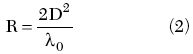
Here, D and λ0 are the maximum aperture and working frequency free space wavelength of the embedded antenna of the radio frequency chip. From the power transfer equation of Friis, the maximum power antenna gain (in front of the center of the dipole antenna) is given by:

Here
Gt and Gr = transmit and receive antenna gain Pt = transmit power Pr = receive power
Again, since the two antennas are the same, Gr = Gt = G. The power ratio Pr/Pt is the measured direct transmission coefficient |S21|2 obtained from the VNA. Figure 8 shows a probe station micrograph of the measurement setup on the wafer. The maximum antenna power gain measured at 60 GHz is approximately -10 dBi. This is in perfect agreement with the simulation conclusions. Table 2 gives a summary of the performance of the antenna radiation characteristics.
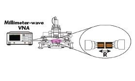
Figure 7 Configuration diagram of the test on the RF chip embedded antenna chip
3. Conclusion
This paper discusses the design, fabrication, and on-wafer measurement of an embedded micropole antenna with an integrated microstrip via-unbalance-balancer, 60 GHz millimeter-wave CMOS RF chip. This is to implement a radio frequency chip embedded system (SoC) for a 60 GHz radio using an integrated low-cost monolithic integrated CMOS RF front-end circuit antenna. The antenna chip is fabricated using a 0.18 micron CMOS process with a chip size of 0.75 × 0.66 mm.
A 3D full-wave EM solver-HFSS based on FEM was used for design simulation. On-wafer measurements were made on the maximum antenna power gain of the input VSWR and the RF chip embedded antenna. The measured antenna VSWR is less than 3 between 55 and 65 GHz. The measured H-plane radiation pattern is approximately an omnidirectional pattern, and the simulated antenna radiation efficiency is approximately 16. This may be caused by CMOS substrate losses. The measured antenna power gain at 60 GHz is about -10 dBi, which is in good agreement with the simulation results. In the future, an integrated product of a 60 GHz RF chip embedded antenna with a 60 GHz CMOS RF front-end circuit will be obtained.
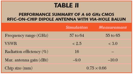
Table 2 Summary of performance of 60 GHz CMOS RF chip embedded dipole antenna with via unbalance-balancer
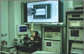
Figure 8 Probe Station Wafer Test Setup
Box Header Connector,Dual Row R-Type Box Header Connector,Box Header Straight Elevator Connector,Smt Box Header 2.0Mm Connector
Dongguan Yangyue Metal Technology Co., Ltd , https://www.yyconnector.com