The rapid advancement of GaN technology has enabled the development of high-performance devices capable of operating at higher power levels, voltages, and frequencies. This progress is particularly evident in the design of power amplifiers (PAs) used in modern communication systems.

As shown in Figure 1, Qorvo’s QPD1013 transistor is built using 0.50 μm GaN-on-SiC technology, which provides excellent thermal performance and reliability. It comes in a cost-effective 6.6 x 7.2 mm DFN package, making it easier to integrate into PCB designs compared to traditional cermet packages. This packaging choice also simplifies the assembly process, reducing overall manufacturing costs.
While Qorvo's GaN transistors are highly efficient, the high RF power levels they handle still result in significant power consumption. Since these components are surface-mount (SMT), careful PCB layout is essential to ensure optimal thermal management. Two different thermal solutions were evaluated—copper-clad via arrays and copper coin technology—and both were tested for effectiveness.
The first method involves using an array of copper-clad vias beneath the ground pad of the transistor, improving heat dissipation. The second approach uses copper coins, which are solid copper blocks embedded in the PCB during manufacturing. These coins allow for more direct heat transfer from the transistor to the PCB carrier. Although many manufacturers have experience with copper-clad technology, copper coin implementation at RF frequencies is still in its early stages and not yet widely adopted.
Transistor measurements were conducted on sample devices assembled on a 20-mil thick Rogers RO4350 substrate. The transistor was biased at 65V and 240mA under static conditions.
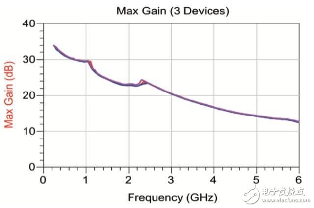
Figure 2 illustrates the maximum usable gain (MAG) of three different transistors across various frequencies, showing good consistency between devices. Although the QPD1013 can operate up to over 6 GHz, practical applications typically limit its operation to around 3.5 GHz due to thermal and stability considerations.
Maximum gain (3 devices) – Maximum gain (dB) – Frequency (GHz)
Load pull measurements revealed that at a 10% duty cycle and 100 μs pulse width, the transistor can deliver over 52 dBm (approximately 160 W) of RF output power with an efficiency of about 70%. This data serves as the foundation for the PA’s large-signal design.
In designing the power amplifier, the first step was to ensure that the transistor remains unconditionally stable across the entire operating frequency band. Stability was achieved by incorporating an RC network at the RF input. Conventional SMT resistors could not handle the power requirements, so high-power aluminum nitride resistors from IMS were used instead. The amplifier must remain stable even at temperatures as low as -40°C to support wide temperature operation. Low-frequency stability was further improved by adding appropriate RC decoupling at the bias feed point, which can be added later in the design phase.
Using initial load pull data provided by Qorvo, the optimal load impedance for maximizing output power and drain efficiency was determined within the 1.2–1.8 GHz range. Under certain load conditions, the QPD1013 can deliver up to 200W, but careful attention to efficiency is necessary to manage transistor temperature. The load impedance corresponding to the highest drain efficiency was selected as the target for the output matching network. This configuration ensures high RF output power while maintaining acceptable thermal performance.
The output matching network employs a bandpass topology to achieve the desired load impedance. High operating voltages and RF power levels pose challenges for designers, requiring careful attention to trace widths to avoid excessive heating or damage. The selection of matching capacitors must also account for their breakdown voltage and quality factor (Q) to minimize losses and maintain efficiency.
The Keysight Momentum tool was used for planar electromagnetic (EM) simulation of the metal parts in the output matching network. Additionally, the multi-port S-parameter block of the O805 SMT component was simulated using its embedded high-frequency model. Figure 3 presents a hybrid EM/schematic diagram of the output matching network.


In Figure 4, the simulated load impedance is plotted on a Smith chart normalized to 10 Ω, overlaying the target impedance. The results indicate that the designed load impedance meets the required power and efficiency specifications.
S(3,3) QPD1013_Opt_Zload_v1..S(1,1)
Frequency (1.200 GHz to 1.9000 GHz)
The analog insertion loss of the output network is shown in Figure 5.

The insertion loss in the output matching network comes from both transmission line losses and losses from SMT components on the PCB. At such high power levels, even small losses can translate into significant power dissipation, directly impacting the overall efficiency of the PA.

Figure 6 shows the EM analog input matching network.
The input matching network uses a low-pass architecture, and IMS aluminum nitride resistors are employed in the gate stability network. These resistors can handle several watts of power, allowing the PA to withstand high input drive levels of 10 to 20W needed for P-3dB compression. Similar to the output network, the input matching network includes inductive loops and pads for post-manufacturing tuning. However, in the final design, only minor adjustments to the capacitance were required.
The analog small signal performance of the PA is illustrated in Figure 7, showing a wide bandwidth and flat gain response across the operating frequency range.

1000W Solar Generator
Super Green Energy Portable Solar Generator Battery Energy Storage System USB Power Station for Outdoor Picnic

1000 Solar Generator,All In One Solar Generator,Outside Home Off grid Portable Solar Generator
suzhou whaylan new energy technology co., ltd , https://www.xinlingvideo.com