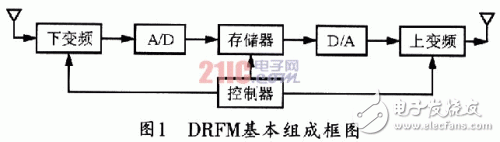
1 DRFM data acquisition module design 1.1 The main features of MAXlOlA ADC chip is the core device of data acquisition, the A/D converter in this system uses MAXIMOlA of MAXIM, its maximum sampling rate can reach 500 Msps, sampling accuracy is 8 bit. This article uses two MAX101A samples alternately to achieve a sampling rate of 1 Gsps. The main features of MAXlOlA are as follows: ◇ has a 500 MHz conversion rate; 有效 has a valid bit of 7.0 at 250 MHz
1 DRFM data acquisition module design1.1 Main features of MAXlOlA
The ADC chip is the core device of data acquisition. The A/D converter in this system uses MAXIMO1A of MAXIM, which has a maximum sampling rate of 500 Msps and a sampling accuracy of 8 bits. This article uses two MAX101A samples alternately to achieve a sampling rate of 1 Gsps. The main features of MAXlOlA are as follows:
â—‡ has a 500 MHz conversion rate;
有效 The effective bit at 250 MHz is 7.0 bits;
â—‡ 1.2 GHz analog input bandwidth;
◇ error is less than ± 1/2LSB INL;
50 with 50 Ω differential or single-ended input;
◇ has an analog input range of ±250 mV;
â—‡Data path can double latch output;
1.2 Principle of MAXl01A
(1) Multi-bit conversion
The MAXl01A uses a parallel architecture (ie, a flicker structure) for faster multi-bit conversion than a normal-integrated ADC. A typical n-bit scintillation structure contains (2n-1) comparators whose negative inputs are evenly spaced from the bottom of the reference network step resistor to the top, each occupying an LSB delta value. The MAXl01A is a monolithic dual-cross parallel quantization chip with two independent 8-bit converters. When n=8, there should be 255 comparators. These converters pass the results to the A and B sets of outputs and latch them on alternate negative edges of the input clock.
(2) Tracking/maintaining
The MAXlOlA's internal tracking/holding amplifier improves the performance of valid data bits and allows analog data to be captured with high accuracy at high slew rates. Its internal Track/Hold circuit provides two important functions for MAXIMA: one is that its 4x nominal gain reduces the amplitude of the input differential voltage, and the input signal is +250mV for a ±1.02 V reference; A differential 50 Ω input is provided to make the MAXl01A interface extremely convenient.
(3) Data flow
The MAXlOlA internal trace/hold amplifier provides the ADC with a sample of the analog input voltage. The T/H amplifier is divided into two parts at the same time, working on the negative edges of the alternate clocks. The input clock CLK should meet the T/H amplifier requirements and can be fed back to the A/D section. The output clock DCLK is used for data timing and is divided by 2 or 10 of the input clock CLK.
1.3 Application of MAXlOlA
(1) Analog input range
Although the normal operating range is +250 mV, for each input of the MAXl01A, its input range to ground is actually ±500 mV, which extends the input level of the voltage including the analog signal and any DC common mode. . To get a full-scale digital output in differential input mode, add +250 mV between AIN+ and AIN-, that is, AIN+=+125 mV, AIN-=-125mV (no DC offset). When there is no voltage difference between the analog inputs, the intermediate scale digital drive will be -250mV, ie AIN+=-125 mV, AIN-=+125 mV, a zero-scale digital output code will appear.
(2) Benchmark
The ADC's reference resistance determines the size and dynamic operating range of the least significant bit (LSB) of the ADC. Typically, the bottom and top of the resistor string are driven by an internal buffer amplifier. The best performance is achieved by adding an RC network to the reference input of the ADC, which connects a 33 Ω resistor to the buffered output stage that drives the reference resistor string, while the 0.47μF capacitor must be connected next to the resistor in the buffered output stage. This resistor-to-capacitor combination must be within 0.5 inches (1.27 cm) of the MAXl01A package. The noise at either termination directly affects the detection of the code and reduces the effective data bit specification of the ADC.
(3) Clock CLK and DCLK
All input and output clocks of the MAXl01A are differential. The input clocks CLK and DCLK are the basic timing signals of the MAXl01A. CLK and DCLK are locked to the internal circuitry by an internal 50 Ω resistor transfer line. Only one pair of CLK and DCLK inputs are driven, while the other paired terminals are connected to -2 V through the 50 Ω transmission line. For a simple circuit connection, any pair of input terminals can be used as the driven terminal. DCLK and /DCLK are the output clocks generated by the input clock for the internal output timing of data packets A and B (Group A data is valid after the rising edge of DCLK. Group B data is valid after the falling edge). In normal mode, they are clock signals that are half the input clock speed. The MAXl01A can operate at input frequencies up to 500 MHz.
(4) Output mode control (DIVl0)
When the DIV10 pin of MAXl01A is grounded, it operates in the detection mode. At this time, the input clock is divided by 10, which reduces the output data and clock frequency to 1/5, but still guarantees that the duty cycle of the output clock is 50%, and the clock connected to the output phase remains unchanged, so every 5 Four of the input sample values ​​are discarded. Conversely, when the DIV10 pin is left floating, it is pulled low by the internal resistor and the MAX-lolA operates in the normal mode.
(5) Wiring, grounding and power supply
For normal operation, MAxl01A requires a +5&TImes; (1 ± 0.01) V positive supply and a -5.2 & TImes; (1 ± 0.01) V negative supply. Bypass the VTT and Vcc supplies with high quality 0.1μF and 0.01μF ceramic capacitors and ground as close as possible to the pins. All ground pins need to be connected to the ground plane to optimize noise immunity and improve application accuracy.
2 data cache module designThe data buffer uses Ahera's FLEXlOKE series CPLD. This design utilizes FLEXlOKE devices for high-speed FIFOs. Since the input and output clock frequencies of FIF0 as data buffers cannot be the same, a dual-clock FIFO must be used. And this type of device is powered by low voltage, which greatly reduces system power consumption and improves system flexibility and reliability.
The system described in this article uses the VHDL hardware description language to program FLEXlOKE. The programming environment is MAX+PLUSIIV9.6.
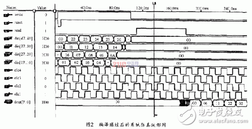
VHDL programming uses a modular design. First, establish 4 modules, namely FIF0, MUX, counterl, counter2. The FIFO can either call lpm-FIF0 (dualClock) to modify some of the key parameters to meet the requirements, or you can manually write the program implementation. Here, the macro module is called. It is worth noting that the input and output clock frequencies of the FIFO are different, so the dual clock FIF0 must be used. MUX, counterl, and counter2 are multiplexers and dividers (counters) used with FIF0, and their source programs should be written by hand. After several sub-modules are completed, a new system module (system) is created to call the sub-modules to complete the definition of the system ports and the logical relationship between the sub-modules in the system module. This design facilitates the integration of logic design to facilitate subsequent improvements. Figure 2 is a waveform diagram of the system simulation after compilation.
This paper takes the DRFM design as the core, and introduces the design ideas and methods of the data acquisition front end of DRFM. In the field of ultra-high-speed data acquisition, the sampling speed of hundreds of megahertz or even 1 GHz is not only domestic, but also the difficulty of circuit design in foreign countries. The use of SRAM-based CPLDs can effectively avoid the high power consumption and high overhead caused by using high-speed FIFOs as buffers. The data cache can be implemented in one chip, reducing the complexity of the hardware and reducing the power consumption of the system. What is more noteworthy is that this kind of CPLD has icr, that is, the circuit can be reconfigured, and the circuit function can be modified by programming it, which lays a good foundation for the subsequent system improvement.
Basic Features
1. The terminal has universal mounting feet so that it can be installed on U-rail NC 35 and G-rail NC32.
2. The closed screw guide hole ensures ideal screwdriver operation.
3. Equipped with uniform accessories for terminals of multiple cross-section grades, such as end plates, grouping partitions, etc.
4. Potential distribution can be achieved by inserting a fixed bridge in the center of the terminal or an edge-plug bridge inserted into the wire cavity.
5. The grounding terminal and the N-line slider breaking terminal with the same shape as the common terminal.
6. Using the identification system ZT, unified terminal identification can be realized.
7. The rich graphics enhance the three-dimensional sense of the wiring system.
Din Rail Terminal Block,Din Rail Fuse Terminal Block,Din Rail Busbar Terminal Block,Din Rail Power Terminal Blocks
Sichuan Xinlian electronic science and technology Company , https://www.sztmlch.com