The microstrip antenna is an antenna formed by attaching a conductor sheet to a dielectric substrate with a conductor ground plate. The antenna has a thin profile, a small volume, a light weight, and is easy to realize multi-band. However, the microstrip antenna has its inherent drawbacks, that is, the broadband is relatively narrow, generally only about 5%. Therefore, it is very important to broaden the bandwidth of the microstrip antenna. At present, with the increasing use of microstrip antennas, many effective methods have been developed for how to widen the bandwidth of antennas. The basic methods are as follows:
(1) increasing the thickness of the microstrip medium;
(2) reducing the dielectric constant of the microstrip medium;
(3) using a lossy medium;
(4) Additional impedance matching network, etc.
The first two methods are relatively simple to manufacture and easy to process; the third method is at the expense of the reduction of the antenna gain; the fourth method requires the design of a broadband matching circuit, which has a complicated circuit structure and is difficult to manufacture.
In this paper, a novel antenna is designed, which uses a thicker air layer and a thinner Teflon double-layer medium. On the basis of the first two methods, the metal capacitor is used to compensate the coaxial probe feed. The introduced inductor simultaneously splits the radiation patch to form a bimodal resonance, further expanding the bandwidth of the antenna. In this paper, the bandwidth of the antenna directly fed by the coaxial probe is compared with the bandwidth of the antenna using only the capacitor compensation feed. The calculation and simulation of the microstrip antenna, adjusting the position and length of the arc-shaped slit, can make the impedance bandwidth of a single circular patch reach 38% or higher in the S-band, which satisfies the requirements of the antenna bandwidth of modern communication.
1 Model structure of microstrip antenna
The model structure of the microstrip patch antenna is shown in Figure 1 and Figure 2. The medium between the radiating patch and the grounding plate is composed of two parts. The lower layer is an air medium with a thickness of h1 and the upper layer is PTFE. For h2, and h1 is much larger than h2, such a combination can increase the thickness of the dielectric layer and equivalently reduce the relative dielectric constant.
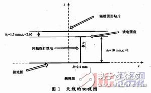
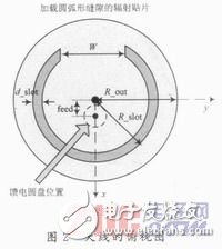
Different from the traditional probe direct feeding, the antenna is loaded with a small circular metal patch on the top of the probe to feed the upper radiating patch. The radius of the capacitor is R, and the position is in the intersection of two layers of media. On the interface. The top layer of the radiation patch does not use a normal circular patch, but instead has a circular groove in its proper position. The radius of the radiation patch is R_out, the outer radius of the arc slot is R_slot, the width is d_slot, the distance between the two ports is W, and the horizontal distance of the feeding coaxial probe from the center of the patch is feed.
2 Theoretical analysis of microstrip antennaThe resonant frequency of a circular microstrip antenna can be approximated by the following equation:
![]()
Where: a is the radius of the circular patch; εr is the effective dielectric constant of the medium.
In general, for a coaxial probe-fed microstrip patch antenna, an increase in the thickness of the dielectric layer causes an increase in inductance caused by the probe, thereby degrading the input impedance of the antenna feed point, which can be caused by the probe. The inductor is compensated. The input impedance of the microstrip antenna and the inductance of the feed probe can be expressed as:
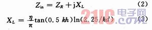
Where: XL is the inductance of the probe; η and k are the characteristic impedance and the wave number in the medium; d is the diameter of the probe. To compensate for the inductance, connect a capacitor in series with the top of the probe and make it meet the resonance conditions:
This effectively optimizes the impedance at the antenna feed point and broadens its impedance bandwidth.
Slotting on the radiating patch can greatly affect the resonant characteristics of the antenna. If the resonant frequency of the slot is not far from the resonant frequency of the patch, the impedance bandwidth of the antenna is likely to be broadened. Common rectangular stickers The form of the loaded U-shaped slot greatly expands the antenna bandwidth. This antenna can also achieve this by using a circular patch to load the arc gap. The following will specifically analyze the effect of the capacitor patch and the slot on the resonance characteristics of the antenna.
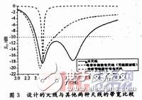
3 related dimensions and resonance characteristics of microstrip antennaCalculate the radius of the circular patch of the antenna resonant frequency at 2.5 GHz using the formula (1) to 21.5 mm, adjust R_out=23 mm, and simulate the position of the feed point feed=6 mm, feed The radius of the disc is R = 2.4 mm, and the arc-shaped slit has R_slot = 16 mm, d_slot = 2 mm, and W = 20 mm.
Figure 3 shows the S11 parameters of the antenna and two other circular microstrip antennas of different structures. The radius of the circular patch is adjusted so that the resonant frequency is around 2.5 GHz. It can be seen from the figure:
Pattern Braided Sleeve,Wire Sleeving,Expandable Braided Sleeving,Cable Wrap Sleeve
Shenzhen Huiyunhai Tech.Co., Ltd. , https://www.cablesleevefactory.com