Summary 
In recent years, LCC resonant converters have attracted much attention because they are superior to conventional series resonant converters and parallel resonant converters: when the load and input vary greatly, the frequency variation is still small, and switching within the full load range can achieve zero voltage conversion. (ZVS). This paper introduces the analysis method of the LLC type resonant converter and reviews the actual design elements of the LLC type resonant converter. This includes designing transformers and selecting components. A design example is used to illustrate the design process step by step, making it easier for engineers to design LLC resonators.
introduction 
In the design of power converters, the requirements for increasing power density and reducing design size are getting higher and higher, and designers are urgently required to increase the switching frequency. The use of high frequency operation will greatly reduce the size of passive components such as transformers and filters. However, the switching losses present have an adverse effect on high frequency operation. In order to reduce the switching loss and make the high frequency work normally, a resonance switching technique is proposed. These techniques process power in a sine wave and the switching device can be easily soft commutated. Therefore, switching loss and noise can be greatly reduced. Conventional resonators use inductive capacitors in series as a resonant network. Load connections have two basic structures, series and parallel.
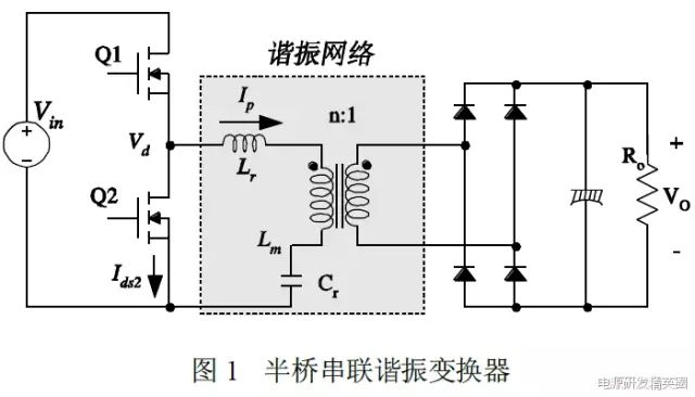
For a series resonant converter (SRC), the rectified load network is connected in series with an LC resonant network, as shown in Figure 1. From this structure, the resonant network acts as a voltage divider with the load. The impedance of the resonant network is changed by changing the frequency of the driving voltage Vd. The input voltage will be distributed to this part of the impedance and reflected load. Because it is a voltage divider, the SRC DC gain is always less than one. Under small load conditions, the load impedance is very large relative to the impedance of the resonant network; all input voltages fall on the load. This makes it difficult to adjust the output under small load conditions. In theory, the output is adjusted without load and the frequency becomes infinite.
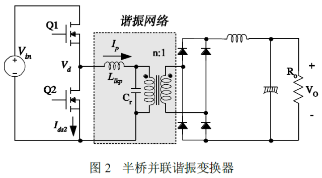
For a parallel resonant converter, the rectified load network and the resonant capacitor are connected in parallel as shown. Since the load is connected in parallel with the resonant network, a large amount of circulating current is inevitably present. This makes it difficult to use a parallel resonant circuit in high power applications.
In order to solve the limitations of the traditional resonant converter, an LLC resonant converter is proposed. Compared to conventional resonators, LLC type resonant converters have many advantages. First, it can adjust the output with a wide range of input and load changes, while the switching frequency changes relatively little. Second, it can achieve zero voltage switching (ZVS) over the entire operating range. Finally, all parasitic components, including the junction capacitance of all semiconductor devices and the leakage inductance and magnetizing inductance of the transformer, are used to implement ZVS.
This article describes the analysis and design elements of a half-bridge LLC resonator. The voltage and current waveforms are analyzed by the fundamental approximation method, and the system gain equation is obtained. A design with a 120W/24V DC/DC converter output is chosen as a typical example to illustrate the design flow.
Working principle and fundamental approximation 
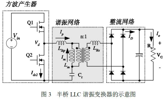
Figure 3 is a simplified schematic of a half-bridge LLC resonant converter, and Figure 4 is a typical waveform. In Figure 3, Lm is the transformer magnetizing inductance, and Llkp and Llks are the leakage inductances of the primary and secondary transformers, respectively. The LLC resonant converter works like a conventional LC series resonant converter. The only difference is that the magnetizing inductance is relatively small, so the resonance between Lm+Llkp and Cr affects the operation of the converter. Due to the small magnetizing inductance, there is a considerable magnetizing current (Im), as shown in Figure 4.
In general, the LLC resonant topology consists of three parts, as shown in Figure 3; a square wave generator, a resonant network, and a rectifying network.
- A square wave generator that generates a square wave voltage Vd by alternately driving switches Q1 and Q2 with a 50% duty cycle with each switching. The square wave generator stage can be designed as a full bridge or a half bridge.
- The resonant network consists of a capacitor, the leakage inductance of the transformer and the magnetizing inductance. The resonant network can filter out higher harmonic currents. Therefore, even if a square wave voltage is applied to the resonant network, substantially only a sinusoidal current is allowed to flow through the resonant network. The current (Ip) lags behind the voltage applied to the resonant network (that is, the fundamental wave of the square wave voltage (Vd) is applied to the totem on the half bridge), which allows the zero voltage to turn on the MOSFET. As can be seen from Figure 4, the MOSFET turn-on voltage is zero when current flows through the anti-parallel diode.
- The rectification network regulates the AC through a rectifier diode and a capacitor to output a DC voltage. The rectification network can be designed as a full bridge or center tap structure with a capacitive output filter.

The filtering function of the resonant network allows us to obtain the voltage gain of the resonator using the classical fundamental approximation principle, assuming that only the fundamental wave of the square wave voltage input to the resonant network contributes to the power transfer to the output. Since the secondary rectifier circuit acts as an impedance transformer, the equivalent load resistance is different from the actual load resistance. Figure 5 shows how to get the equivalent load resistance. The primary circuit is replaced with a sinusoidal current source Iac and a square wave voltage VRI as the rectifier input voltage. Since the average value of Iac is the output current Io, you can get:


Using the equivalent load impedance, the AC equivalent circuit is obtained. As shown in Fig. 6, VdF and VROF represent the fundamental wave of the driving voltage Vd and the reflected output voltage VRO(nVRI), respectively.

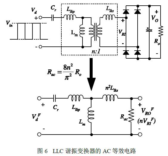
The LLC resonant converter characteristics are obtained using the equivalent load impedance of equation (5). Calculate the voltage gain M using the AC equivalent circuit shown in Figure 6.

As can be seen from equation (6), the circuit has two resonant frequencies. One is determined by Lr and Cr, and the other is determined by Lp and Cr. In the actual transformer, Lp and Lr are measured at the primary using open and short circuits of the secondary coil, respectively.
Equation (6) needs to be concerned that at the resonant frequency (ωo), the gain is fixed regardless of the load.

Regardless of the leakage inductance of the transformer secondary, the gain of equation (7) becomes 1. In previous studies, the leakage inductance of the transformer secondary was often ignored to simplify the gain equation. However, it can be seen that if the secondary leakage inductance of the transformer is ignored, there is a considerable error in the calculated gain, resulting in an incorrect design result.

The gain at the resonant frequency (ωo) in equation (7) can also be reduced to the equation expressed by K.

Although the gain is expressed as equation (8), the gain is preferably expressed as a function of Lp and Lr when operating an actual transformer. Because these two quantities are very easy to measure. Let Lp and Lr be represented by K, we can get:

Using the resonant frequency gain calculated by equation (15) as a virtual gain of the transformer, the AC equivalent circuit of the LLC resonator shown in Figure 6 can simplify the form containing only Lp and Lr, as shown in Figure 7.
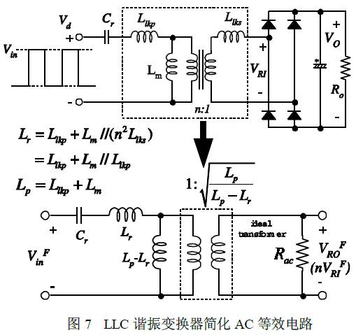
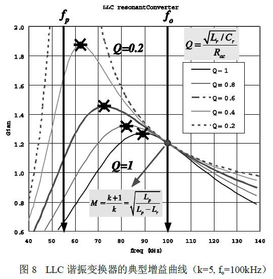
Figure (8) shows the gain of equation (8) for different Q values, where k = 5, fo = 100 kHz and fp = 55 kHz. It can be seen from Figure 8 that when the switching frequency is approximately equal to the resonant frequency fo, the characteristics of the LLC resonator are almost independent of the load. This is a unique advantage of the LLC type resonant converter compared to conventional series resonant converters. Therefore, it is best to operate the converter around the resonant frequency to reduce variations in switching frequency under small load conditions.
The operating range of the LLC resonant converter is limited by the peak gain (maximum achievable gain), which is the position indicated by '*' in Figure 8. It should be noted that the peak voltage gain does not occur in fo nor fp. The peak gain frequency corresponding to the peak gain is between fp and fo, as shown in Figure 8. As the Q value decreases (load reduction), the peak gain frequency moves toward fp and the peak gain is higher. As the Q value rises (the load increases), the peak gain frequency is biased toward fo and the peak gain is decreased. Therefore, the full load state should be the worst case to consider for resonant network design.
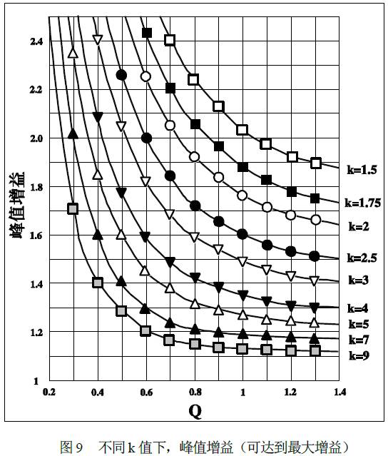
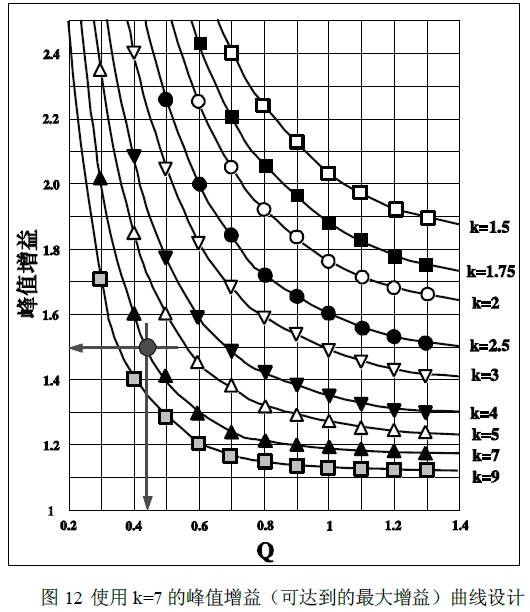
Another important factor in determining the peak gain is the ratio between Lm and Llkp, which is the K value defined in equation (9). Even if the peak gain under a certain condition can be obtained by the equation (8), it is difficult to express the peak gain in a very compact form. Further, for the frequency below the resonance frequency (fo), the gain obtained from the equation (8) has a certain frequency error because of the basic approximation. To simplify analysis and design, peak gain can be obtained by using a simulation tool. Figure 9 illustrates how the peak gain (the maximum gain that can be achieved) varies with Q for different k values. From this point of view, lowering the K or Q value results in a higher peak gain. For a given resonant frequency (fo) and Q value, lowering K means reducing the magnetizing inductance, resulting in an increase in circulating current. Therefore, there is a need to make a compromise between the available gain range and conduction losses.
Design Flow 
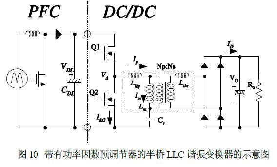
In this section, the design flow is described using the schematic of Figure 10 as a reference. Choose a DC/DC converter with an output of 125W/24V as a design example. The design specifications are as follows:
- Input voltage: 380Vdc (PFC level output)
- Output: 24V/5A (120W)
- Keep time requirement: 17ms
- DC link capacitance at the PFC output: 100uf
[First step] Defining system parameters
The first step must define the following parameters.
Estimated Efficiency (Eff): Estimated power conversion efficiency is mainly used to calculate the maximum input power at a certain maximum output power. If there is no reference value available, Eff is generally 0.88~0.92 for low voltage output applications and 0.92~0.96 for high voltage output applications. With estimated efficiency, you can calculate the highest input power

- Input voltage range (Vinmin and Vinmax): Normally, the input voltage is assumed to be provided by a power factor correction (PFC) pre-regulator output. When the PFC output provides an input voltage, considering the hold time requirement, the minimum input voltage is

Where VO.PFC is the PFC rated output voltage, THU is the hold time, and CDL is the DC link bulk capacitor.
The maximum input voltage is:

[Step 2] Determine the maximum and minimum voltage gain of the resonant network
In the last section, in order to minimize switching frequency variations, LLC resonant converters typically operate near the resonant frequency (fo). When the input voltage is supplied by the PFC input, the input voltage has a maximum value (PFC rated output voltage) during normal operation. The operating frequency at the maximum input voltage of the converter is designed as the resonant frequency (fo), and the minimum gain should occur at the resonant frequency (fo). From equation (11), the fo gain is a function of the ratio between the magnetizing inductance and the primary magnetic flux leakage inductance (k = Lm / Llkp). Therefore, the appropriate k value must be chosen to obtain the minimum gain. However, a small k value still achieves a higher peak gain, and a too small k value makes the transformer poorly coupled and inefficient. Generally, k takes 5~10, and the gain at the resonant frequency (fo) is 1.1~1.2. When the value of k is determined, the minimum voltage gain at the maximum input voltage (Vinmin) can be determined.
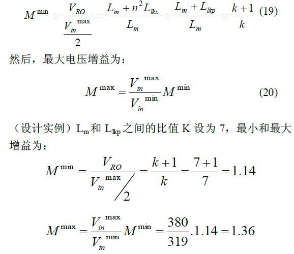

[Step 3] Determine the transformer turns ratio (n=Np/Ns)
Because the rectifier network uses a full-wave bridge rectifier, the transformer turns ratio is:

Among them, VF is the voltage drop of the secondary rectifier diode.

[Step 4] Calculate the equivalent load impedance (Rac)
Calculate the turns ratio of the transformer using Equation 21 and calculate the equivalent load impedance.

[Step 5] Designing a resonant network
Using the K value selected in the second step, read the appropriate Q value from the peak gain curve of Figure 9 to ensure sufficient peak gain. Generally, there is a 10 to 15% margin in the peak gain. Then, you can calculate the resonance parameters
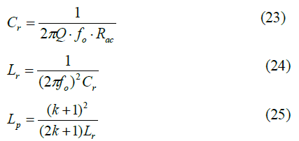

[Sixth Step] Designing a Transformer
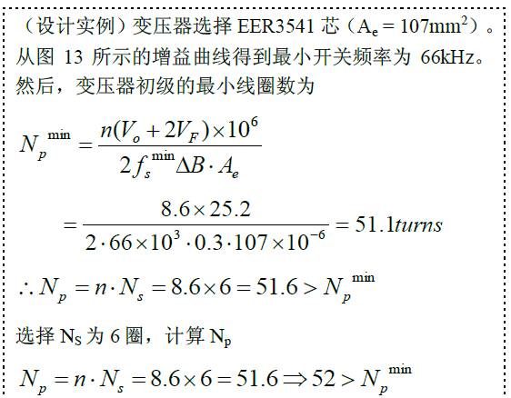
The worst case for transformer design is the lowest switching frequency condition, which occurs at the lowest input voltage and full load. To calculate the lowest switching frequency, draw the gain curve using equation (8) and read the minimum switching frequency. Then, calculate the primary minimum number of coils of the transformer using the following equation

Among them, Ae is the cross-sectional area of ​​the transformer core, the unit m2, △B is the maximum swing of the magnetic flux density, the unit is special. If there is no reference data, △B can take 0.25~0.3T
Then, select the number of secondary coils to ensure that the number of primary coils is greater than Npmin


[Step 7] Transformer construction
In the fifth step, the parameters Lp and Lr of the transformer are determined. Lp and Lr can be measured at the primary by using the secondary coil open and short, respectively. Since the LLC converter design requires a relatively large Lr, a combinable spool is typically used, as shown in Figure 14, to achieve the desired Lr value. For this combinable spool, the number of coils and the winding structure are the main factors determining the Lr size, and the air gap length of the transformer core does not affect the Lr too much. However, Lp can be easily controlled by adjusting the length of the air gap. Table 1 shows the Lp and Lr values ​​measured at different air gap lengths. Assuming an air gap length of 0.15 mm, Lp and Lr values ​​can be obtained.


Even in the LLC resonant converter design, this integrated transformer approach concentrates the magnetic components into a single core, saving a magnetic component, but Lr is not easily controlled in actual transformer designs. Therefore, designing a resonant network sometimes requires the Lr value actually measured after the transformer is manufactured. Or add a resonant inductor in series with the resonant capacitor to get the ideal Lr value.
[Step 8] Selecting the resonant capacitor
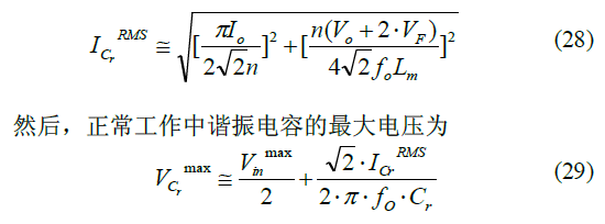
When selecting a resonant capacitor, the rated current must be considered because a significant amount of current flows through the capacitor. The rms current through the resonant capacitor is

in conclusion 
This paper describes the design process of an LLC resonant converter that utilizes the magnetizing inductance and leakage inductance of a transformer as resonant components. When calculating the gain, the leakage inductance of the transformer secondary is considered.
Laptop Stands And Risers,Laptop Riser Computer Laptop Stand,Laptop Folding Table Stand Aluminum,Laptop Stand Portable Aluminum Laptop Riser
Shenzhen ChengRong Technology Co.,Ltd. , https://www.laptopstandsuppliers.com