Low temperature co-fired ceramic (LTCC) technology is a new multi-layer substrate process technology that emerged in the mid-1980s. Low temperature co-fired ceramic (LTCC) uses a unique material system, so its sintering temperature is very low, and it can be combined with metal conductors. Co-firing greatly improves the performance of electronic devices.
This paper designs a miniaturized, low-noise amplifier for wireless local area networks using the advantages of low temperature co-fired ceramic (LTCC) technology. In fact, low-noise microwave amplifiers (LNAs) are currently used in microwave communications, GPS receivers, remote sensing remote control, radar, electronic countermeasures, radio astronomy, geodetic mapping, television, and various high-precision microwave measurement systems, and With the development of industrial technology, its miniaturization technology has also received more and more attention.
1 LTCC's technical advantagesCompared to conventional FR4 sheets, LTCC substrates have significant high frequency advantages. Due to its three-dimensional multi-layer integration function, LTCC has a significant advantage in volume compared to conventional microwave plates (mainly Teflon PTFE). In addition, LTCC materials have a wide range of dielectric constants and can be adapted to the application needs of various frequency bands. Compared with HTCC, due to the low sintering temperature of LTCC, it is possible to use low-melting, low-loss conductor pastes of silver and gold for wiring printing, which greatly reduces the loss of LTCC products; and is very close to the thermal expansion coefficient of semiconductor processes. , more conducive to active / passive integration. In summary, LTCC technology has the following advantages:
LT LTCC materials have excellent high-frequency and high-Q characteristics, and can be used up to several tens of GHz, which can meet the requirements of increasingly advanced RF microwave applications.
â—‡ Using high-conductivity metal materials such as silver, gold, copper and their alloys as conductor materials, it is beneficial to improve the quality factor of the circuit system, and the fabricated circuit conductor loss is small;
â—‡ High integration, low temperature co-fired ceramics (LTCC) can make circuit boards with high number of layers, generally can reach dozens or even hundreds of layers, and can embed multiple passive components, and can integrate components. There are many types and a large range of parameters. In addition to L/R/C, LTCC can integrate sensitive components, EMI suppression components, circuit protection components, etc., and can be surface-applied to active devices/chips for active/passive integration. Assembly density of the circuit;
â—‡ It can adapt to high current and high temperature resistance requirements, and has better thermal conductivity than ordinary PCB circuit substrates;
â—‡ High reliability, high temperature resistance, high humidity, vibration, can be used in harsh environments, such as military communications equipment, aerospace electronics, automotive electronics, etc.;
较低 Low cost, which is a discontinuous production process that allows the inspection of raw ceramic substrates to improve yield and reduce production costs.
2 overall design2.1 Low Noise Amplifier Design Principle
The difference between a low-noise amplifier and a general-purpose amplifier is that the low-noise amplifier is best matched by noise rather than the maximum gain point, so the gain is relatively reduced. The gain in the case of the best noise match is called the correlation gain. Usually the correlation gain is about 2 to 4 dB lower than the maximum gain.
2.2 Performance Specifications, Device Selection and Single Stage Circuit Simulation
This design uses two-stage amplification. The index requirements are as follows: noise figure ≦0.8dB; gain ≧24dB; gain flatness is ±0.5dB; input and output standing wave ≦1.3, and DC~14GH is stable.
When designing, the first stage amplifier can be selected with ATF55143, which has the advantages of high gain, small noise figure, small volume, small working current, stable static working point and less self-excitation. The substrate is made of Ferro's A6 diaphragm and takes into account the built-in inductance, capacitance and mechanical strength. The thickness of the circuit board is 0.6mm.
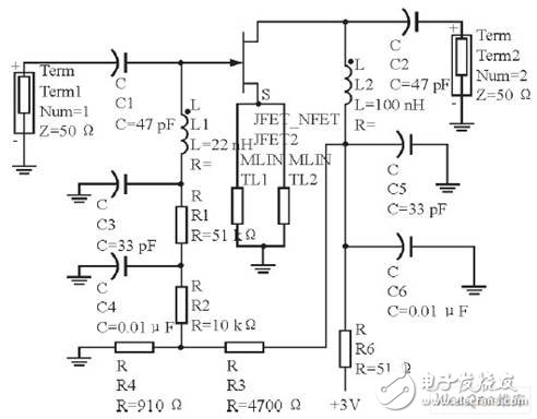
A schematic diagram of the first stage biasing and matching circuit is shown in FIG.

Figure 1 Schematic diagram of the first stage bias and matching circuit
In Figure 1, the reasonable choice of C1, L1, C2, and L2 plays a very important role in whether the noise, S11, S22, gain, etc. can reach the index. These two sets of L/C high-pass filter circuits can also effectively suppress low-frequency oscillations. The reasonable choice of R1 and R2 not only reduces the leakage current, but also stabilizes the low frequency signal.
The C3 and C6 bypass capacitors provide filtering and stabilization. R3 and R4 are used to provide a suitable turn-on voltage for the gate.
Source-level series negative feedback plays a pivotal role in the stability of the full-band. These two microstrip lines are equivalent to a small inductor in series, which has the advantages of simplicity, convenience, cost reduction, and ease of debugging. The circuit can skillfully combine the bias circuit with the input and output circuits through proper matching and negative feedback, which not only saves space but also reduces the device and saves cost.
The second stage of this design uses RFMD's monolithic amplifier SPF-5O43Z, which has the advantages of small size, easy miniaturization, low noise, simple power supply circuit, and good stability. Both amplifiers are powered from a single supply, with low supply voltage and low current for easy adjustment.
2.3 Debugging and optimization of two-stage circuit
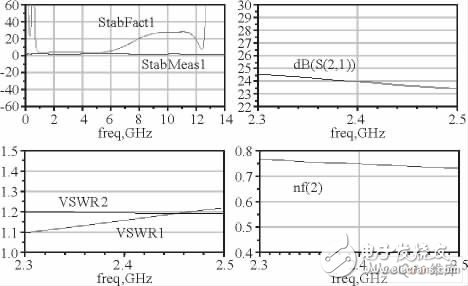
The difficulties encountered in the process of combining and debugging two-stage circuits are mainly due to the stability and the possibility that the input standing wave may not reach the standard. After the simulation, many places will not meet the actual requirements. For example, the values ​​of capacitors, inductors, and resistors may not meet the actual needs, and the line width is too narrow. Therefore, after copying a single-stage circuit, if you simply connect the circuits at each level, you will often fail to meet the specifications. Figure 2 shows the simulation results of its overall circuit.

Figure 2 Overall circuit simulation results
Single Phase Isolation Transformer
Generally included
Single Phase Isolation Transformer,Isolation Transformer,Auto Transformer,Single Phase Electrical Transformer
Characteristic
1. Anti interference effect: if the isolation transformer connected with Y/â–³ can prevent the transmission of some harmonics;2. Impedance transformation function: increase the system impedance, so that the protection device can be easily matched;
3. Function of stabilizing system voltage: for example, when starting heavy load equipment, reduce the impact on system voltage;
4. Function of preventing system grounding: when single-phase grounding occurs on the load side of the isolation transformer, it will not cause single-phase grounding of the whole system (above the Satons isolation transformer);
5. Reduce short circuit current: limit the short circuit current of the system when a short circuit accident occurs on the load side.
DG (B) /BK series single-phase isolation transformer can not only change the voltage, but also electrically isolate the input winding and output winding from each other, so as to avoid the danger caused by touching electrified body (or metal parts that may be electrified due to insulation damage) and ground at the same time. In addition, the isolation transformer also has the function of restraining various inter ferences.
Product performance
Input voltage 220v can be customized according to requirements, and output voltage 110v, 127v, 200v, 208v can be customized according to requirements Voltage stabilization accuracy ± 1% Output no-load current ≤ 2% Frequency 50hz/60hz Withstand voltage 2m Ω Waveform harmonic 1500v Voltage 1 min No breakdown and flash over Withstand voltage f Maximum temperature rise 150 ℃
Single Phase Isolation Transformer,Isolation Transformer,Auto Transformer,Single Phase Electrical Transformer
Henan New Electric Power Co.,Ltd. , https://www.newelectricpower.com