1. If the FPGA system is designed in the circuit system, the Quartus II software must be used to verify the pin assignment before drawing the schematic. (Some special pins in the FPGA cannot be used as normal IO)
2, 4 layers from top to bottom are: signal plane layer, ground, power, signal plane layer; 6 layer board from top to bottom are: signal plane layer, ground, signal inner layer, signal inner layer, Power Supply, signal plane layer. More than 6 layers (the advantage is: anti-interference radiation), the inner layer is preferentially selected, the plane layer is not selected, and the ground or power layer is prohibited from being routed (cause: the power layer will be split and parasitic effects will be generated).
3, multi-power system wiring: such as FPGA + DSP system to do 6-layer board, generally at least 3.3V +1.2V +1.8V +5V.
3.3V is generally the main power supply, directly laying the power layer, and it is easy to pass through the global power network through the via. 5V is generally a power input and only needs to be copper in a small area. And as thick as possible (you ask me how thick it is - how thick it is, how thick it is, the thicker the better)

1.2V and 1.8V are core power supplies (if direct connection is used, it will be very difficult to face BGA devices). When layout, try to separate 1.2V from 1.8V and connect it to 1.2V or 1.8V. The components are arranged in a compact area, connected by copper, as shown below:

In short, because the power network is spread over the entire PCB, if the way of routing is complicated and will go very far, the method of using copper plating is a good choice!
4. The crossover between the adjacent layers is used to reduce the electromagnetic interference between the parallel wires (high school) and to facilitate the routing (Ref. 1). The following figure shows the traces of two adjacent layers in a PCB, which is roughly one horizontal and one vertical.


5, analog digital to be isolated, how to isolate? When the layout of the device used for analog signals and digital signal devices, and then cut from the middle of the AD chip!

The analog signal is grounded analog, and the analog ground/analog power supply is connected to the digital power supply through a single point of the inductor/bead.

6. PCB design based on PCB design software can also be regarded as a software development process. Software engineering pays most attention to the idea of ​​“iteration developmentâ€. I think this idea can also be introduced in PCB design to reduce the probability of PCB errors. (1) Schematic check, paying particular attention to the power supply and ground of the device (the power supply and ground are the blood vessels of the system, there must be no negligence) (2) PCB package drawing (confirm whether the pins in the schematic are incorrect) (3) PCB After confirming the package size one by one, add the verification label, add it to the design package library (4), import the net list, and adjust the signal sequence in the schematic while layout (the automatic numbering function of OrCAD can no longer be used after the layout) (5) Manual Wiring (checking the power supply network on the side of the cloth, as mentioned earlier: the power supply network uses copper plating, so use less wiring.) In short, the guiding idea in PCB design is to draw the package layout and feedback correction schematic (from the signal connection) The correctness and convenience of signal routing are considered).
7, the crystal oscillator is as close as possible to the chip, and the crystal oscillator should not be routed as much as possible, paving the network copper. The clocks used in multiple places are routed using a tree clock tree. 8. The arrangement of the signals on the connector has a great influence on the ease of wiring. Therefore, adjust the signal on the schematic while wiring (but never renumber the components)
9, multi-board connector design:
(1) Use Cable connection: the upper and lower interfaces are consistent. (2) Straight Socket : The upper and lower interfaces are mirror-symmetrical, as shown below.

10, the module connection signal design: (1) If two modules are placed on the same side of the PCB, as follows: the discipline number is large and small (large mirror connection signal)

(2) If two modules are placed on different sides of the PCB, the management number is small and small, so that the signal can be placed as if it is the same as the right image above. Of course, the above method is not a rule. I always say that everything changes with the needs (this can only be understood by myself), but in many cases, designing in this way is very useful.
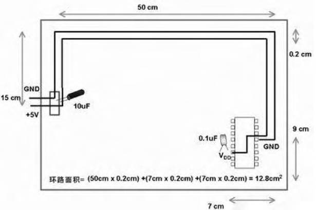
11, the design of the power ground circuit:

The power ground circuit of the above figure has a large area and is susceptible to electromagnetic interference.

The above figure is improved by the fact that the power supply and ground are close to the trace, which reduces the loop area and reduces electromagnetic interference (679/12.8, about 54 times). Therefore, the power supply and ground should be as close as possible to the traces; and between the signal lines should avoid and walk the line as much as possible to reduce the mutual inductance effect between the signals.
If you are desperately looking for a safe, portable power charger for different brands laptop, spare or for travel with multiple devices, this is the one for you--universal Laptop Charger.
Yidashun offer manual and automatic universal laptop Adapter. Universal power adapter have 40W 70W 80W 90W 100W 120W 150W with home and car use. Usually one charger with 8 standard interchangeable dc tips makes it compatible with most brands of different laptops, of course you can also add extra more tips as you want.
For manual universal ac adapter, you need to set the switch to right voltage and plug in right dc tip for your laptop, or it won`t charge well. But for automatic universal power supply, only if you plug into right dc tip according to your laptop, it charges your laptop very well right now, no need you to set the voltage, it is much easier for you to use.


Universal Laptop Charger,Universal Computer Charger,Universal Laptop Adapter,Universal Wall Plug Adapter
Shenzhen Yidashun Technology Co., Ltd. , https://www.ydsadapter.com