Introduction
In fiber optic telecommunications systems, laser diodes are used as transmitting lasers for transmitting signals, as well as pump lasers for erbium doped fiber amplifiers (EDFAs) and optical amplifiers (SOAs). In these applications, the characteristics of the laser (including wavelength, average optical power, efficiency, and extinction ratio) must be stable to ensure good overall performance of the telecommunications system. However, these characteristics depend on the temperature of the laser: as long as the temperature drifts, the wavelength changes and the conversion efficiency will decrease. The required temperature stability is between ±0.001 °C and ±0.5 °C, depending on the application.
To control the temperature, a loop consisting of a thermistor, a thermoelectric cooler (TEC), and a TEC controller is required. The thermistor's resistance varies in proportion to temperature (inverse or proportional, depending on the thermistor type), which can be used to convert temperature to voltage when configured as a voltage divider. The TEC controller compares the feedback voltage to a reference voltage representative of the target temperature and then controls the current flowing through the TEC to adjust the amount of heat transferred by the TEC.
A general block diagram of the above system is shown in Figure 1. The laser diode, TEC and thermistor are located inside the laser module. The TEC controller ADN8833 or ADN8834 reads the feedback voltage of the thermistor and provides the drive voltage to the TEC. Use a microcontroller to monitor and control the thermal loop. Note that the thermal loop can also be built in an analog circuit. The ADN8834 has two zero-drift chopper amplifiers that can be used as PID compensators.
This article will explain the composition of the laser diode thermal control system in a telecommunications system and introduce the key specifications of the main components. The purpose of this paper is to present various design considerations from a system perspective, providing a global guide for designers to build a high-performance system with good temperature control accuracy, low loss, and small size.
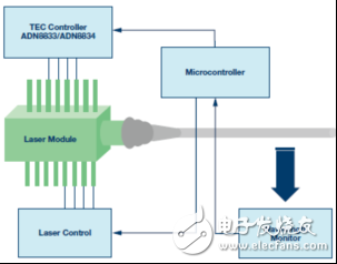
Figure 1. Temperature control system for the laser module
TEC: Thermoelectric Cooling Technology
The thermoelectric cooler includes two surface ceramic plates with P-type and N-type semiconductor arrays alternately placed as shown in FIG.
When current flows through these conductors, heat is absorbed at one end and released at the other end; when the current is in the opposite direction, heat transfer is reversed. This process is called the Peltier effect. The carriers in the N-type semiconductor are electrons, and therefore, carriers and heat flow from the anode to the cathode. The opposite P-type semiconductor has hole carriers, and heat also flows in the opposite direction.
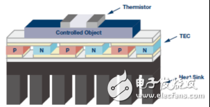
Figure 2. TEC module with heat sink
Take a pair of PN semiconductor pairs and connect them with a metal plate, as shown in Figure 3. When current flows, heat is transferred in one direction.
Changing the polarity of the DC voltage changes the direction of heat transfer, and the amount of heat transferred is proportional to the magnitude of the voltage. Because of its simplicity and robustness, thermoelectric cooling is widely used for thermal conditioning of telecommunications systems.
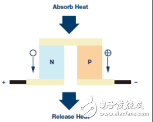
Figure 3. Peltier effect: heat flow of a PN semiconductor pair
Select TEC module
When choosing a TEC module, you need to consider many factors in the system, such as ambient temperature, target temperature, heat load, power supply voltage, and physical characteristics of the module. The thermal load must be carefully evaluated to ensure that the selected TEC module has sufficient capacity to pump heat away from the system to maintain the target temperature. TEC module manufacturers typically provide two performance curves in the data sheet. One curve shows the heat transfer capacity at different temperature differences (ΔT) over the supply voltage range, and the other curve shows the cooling/heating current required for different combinations of supply voltage and ΔT. The designer can estimate the power capacity of the module to determine if it meets the needs of a particular application.
TEC controller operation and system design
To compensate for temperature with TEC, the TEC controller should be able to generate a reversible differential voltage based on feedback error and provide appropriate voltage and current limits. Figure 4 shows a simplified system block diagram of the ADN8834. The main functional modules include temperature sensing circuits, error amplifiers and compensators, TEC voltage/current detection and limit circuits, and differential voltage drivers.
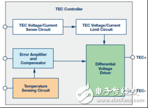
Figure 4. Functional block diagram of the single-chip TEC controller ADN8834
Differential voltage driver
The TEC controller outputs a differential voltage such that the current through the TEC can carry away the heat of the object connected to the TEC or smoothly change to the opposite polarity to heat the object. The voltage driver can be a linear mode, a switch mode, or a hybrid bridge. Linear mode drives are simpler and smaller, but not efficient. Switch mode drivers have good efficiency - up to 90% - but the output requires additional filter inductors and capacitors. The ADN8833 and ADN8834 use a hybrid configuration with a linear driver and a switch-mode driver that halve the number of larger filter components while maintaining high efficiency.
The voltage driver design is critical to the controller because it takes up most of the power and board space. Optimized driver stages help minimize power loss, circuit size, heat sink requirements and cost.
Detect temperature with NTC thermistor
Figure 5 shows the impedance of the negative temperature coefficient (NTC) thermistor over the temperature range. Because it is temperature dependent, it can be connected as a voltage divider to convert temperature to voltage. A typical connection is shown in Figure 6. When RTH changes with temperature, VFB also changes. Adding an Rx in series with the thermistor linearizes the temperature-to-voltage transfer function relative to VREF, as shown in Figure 7. It must be tightly coupled to the laser inside the module housing to isolate the effects of external temperature fluctuations, allowing it to accurately detect temperature.

Figure 5. NTC impedance vs. temperature 
Figure 6. NTC thermistor is connected as a voltage divider to convert temperature to voltage 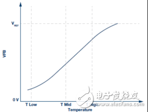
Figure 7. Relationship between VFB and temperature
Error amplifier and compensator
The analog thermal feedback loop consists of two stages, consisting of two amplifiers, as shown in Figure 8. The first amplifier accepts a thermal feedback voltage (VFB) that is converted or regulated to a linear voltage output. This voltage represents the temperature of the object and is fed into the compensation amplifier and compared to the temperature set voltage to produce an error voltage that is proportional to the difference between the two. The second amplifier is typically used to construct a PID compensator that includes a very low frequency pole, two different higher frequency zeros, and two high frequency poles, as shown in Figure 8.
The PID compensator can be determined mathematically or empirically. To mathematically simulate a thermal loop, the exact thermal time constant of the TEC, laser diode, connector, and heat sink is required, which is not readily available. It is more common to tune the compensator using empirical methods. By assuming that the temperature set-end has a step function and changes the target temperature, the designer can adjust the compensation network to minimize the settling time of the TEC temperature.
The aggressive compensator reacts quickly to thermal disturbances, but it can easily become unstable, while the conservative compensator builds up slowly, but withstands thermal disturbances and is less likely to overshoot. A balance must be struck between system stability and response time.

Figure 8. Thermal feedback loop diagram using two internal chopper amplifiers in the ADN8834
Key performance of the TEC controller system
Temperature adjustment accuracy
Sometimes, even if the PID compensator is properly designed, steady-state errors will still exist. The following are a few factors that can cause this error.
TEC Thermal Power Budget: When designing the system, the TEC and supply voltage were the first choices. However, since the thermal load is not easy to estimate, the choice may not be correct. In some cases, if the maximum power is applied to the TEC but the target temperature is still not reached, it may mean that the thermal power budget is not sufficient to handle the thermal load. Increasing the supply voltage or selecting a TEC with a higher power rating can solve this problem.
• Voltage Source Consistency: The reference voltage drifts with temperature and time, which is usually not a problem for closed thermal loops. However, especially in digital control systems, the TEC controller and the microcontroller's reference voltage source may have different drifts, causing errors that the compensator does not notice. It is recommended that these two circuits use the same reference source and cover the other voltage with a voltage with a higher drive capability.
• Temperature detection: To minimize temperature error, it is important to accurately measure the load temperature. Any error from the feedback will enter the system, and the compensator will not be able to correct this error. Use high precision thermistors and auto-zero amplifiers to avoid errors. The arrangement of the thermistor is also important. Be sure to mount it on the laser so that you can read the actual temperature we want to control.
effectiveness
Most of the power consumption of the TEC controller is consumed by the driver stage. In the ADN8833/ADN8834, the linear driver's power dissipation is directly derived from the input-to-output voltage drop and load current. Switch mode driver losses are complex and can be roughly broken down into three parts: conduction loss, switching loss, and conversion loss. The conduction loss is proportional to the RDSON of the FET and the DC resistance of the filter inductor. Selecting a low-resistance component reduces conduction losses. Switching losses and switching losses are highly dependent on the switching frequency. The higher the frequency, the higher the loss, but the passive component size can be reduced. In order to achieve optimal design, we must carefully weigh efficiency and space.
Noise and ripple
The switch mode driver in the ADN8833/ADN8834 switches at 2 MHz, and the fast PWM switching clock edge contains a wide spectrum that produces voltage ripple at the TEC terminal and produces noise throughout the system. Adding proper decoupling and ripple rejection capacitors reduces noise and ripple.
For the buck topology commonly used in switch mode power supplies, the ripple on the supply voltage rail is mainly caused by the intermittent current of the PWM FET chopping. Using multiple SMT ceramic capacitors in parallel reduces the ESR (equivalent series resistance) and decouples the supply voltage locally. At the output of the switch mode driver, the voltage ripple is caused by the current ripple of the filter inductor. To suppress this ripple, multiple SMT ceramic capacitors should be used in parallel between the driver output and ground. The ripple voltage is mainly determined by the product of the capacitance ESR and the inductor ripple current: ΔV_TEC = ESR &TImes; ΔI_L uses multiple capacitors in parallel to effectively reduce the equivalent ESR.
in conclusion
Designing a TEC controller system for laser diodes in a telecommunications system is a complex task. In addition to the thermal accuracy challenges, package sizes are typically very small and power consumption tolerances are low. In general, a well-designed TEC controller should have the following advantages:
? Precision temperature adjustment
? high efficiency
? The board size is small
? Low noise
? Current and voltage monitoring and protection
3520 Phenolic Paper Laminated Tube is formed by hot rolling, baking insulation paper impregnated with phenolic resin under heat and pressure. It is class E (120℃) insulation with high mechanical property. It has good dielectric property in dry conditions.
It is suitable for structural parts of electrical equipments in dry conditions and transformer oil.
Product diameter Φ5mm-Φ5000mm, product length> 20mm or more optional, product wall thickness> 3mm or more optional, product shape cylindrical tube, square tube, hexagonal tube, special-shaped tube, oval tube.
Phenolic Tube,Phenolic Paper Tube,Laminated Paper Tube,Laminated Phenolic Paper Tube
Yingkou Dongyuan Electrical Insulation Board Co.,Ltd , https://www.dy-insulation.com