In the study of electronic information systems, we are often told that the real world is analog, while the digital world is becoming increasingly sophisticated. However, the distinction between numbers and simulations is relative. You can think of analog signals as a continuous stream of infinite values, or you can consider digital representations as discrete samples with varying spacing. The difference between these two approaches lies in the processes of sampling and quantization!
So, how does an analog signal get converted into a digital one?
**First, the steps of ADC (Analog-to-Digital Conversion)**
1. **Sampling and Holding**
If we compare analog signals to digital ones, which require infinite sampling points, we need to take a finite number of samples for accurate digital transmission. The question is: how many samples do we take, and how do we choose them?
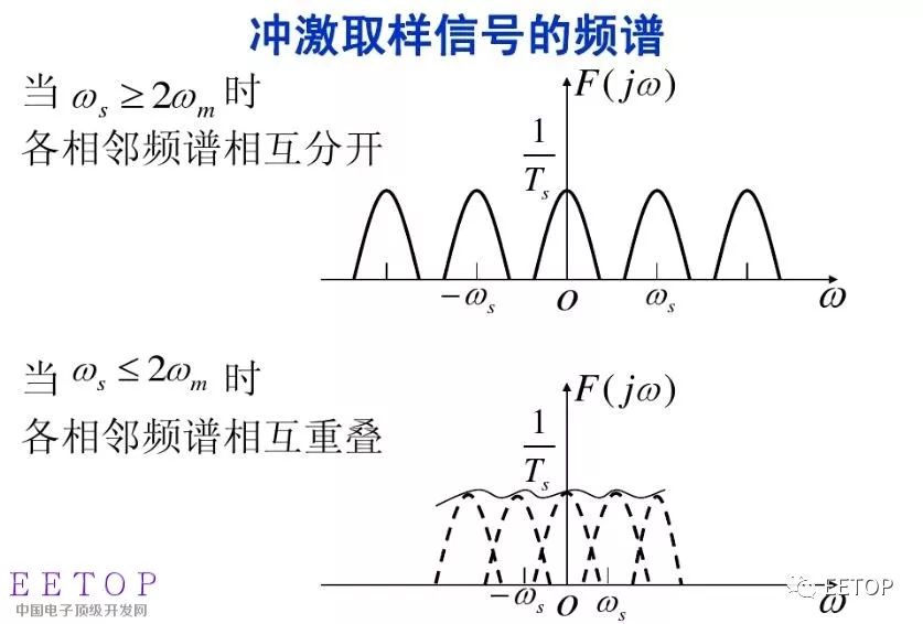
The Nyquist Sampling Theorem states that the sampling frequency must be at least twice the highest frequency component of the signal (fs ≥ 2fn). This ensures that the original signal can be reconstructed without distortion. If this condition isn't met, aliasing occurs, where high-frequency components appear as lower frequencies. A visual representation of the spectrum is shown below.
The purpose of holding is to store the sampled value for the next stage of processing.
2. **Quantization and Coding**
Quantization involves converting the sampled values into binary digits (0s and 1s) based on specific standards and steps. Different ADC architectures achieve this in various ways, each with unique performance characteristics.
**Second, Several ADC Architectures**
1. **Integrating ADC**
As the name suggests, integrating ADCs use an operational amplifier to integrate both the input and reference signals. The reference signal is typically opposite in polarity to the input, causing the output voltage to rise and fall over time. A counter measures this time interval to determine the sampled value.
Features:
- High accuracy but low speed.
- Strong noise immunity due to integration.
- Rarely used in modern designs due to its limitations.
2. **Successive Approximation Register (SAR) ADC**
This type of ADC uses a comparator to compare the input signal with a reference generated by a DAC. It starts with a mid-scale value and adjusts the bits sequentially until it converges on the correct digital value.
Features:
- Medium speed (100K–1M samples per second).
- Medium resolution (12–16 bits).
- Widely used due to its good balance of speed, power, and performance.
- Requires precise DAC calibration and fast comparator.
3. **Pipeline ADC**
This architecture uses multiple stages of comparators working in parallel, making it extremely fast. Each stage processes a portion of the signal, passing the result to the next stage.
Features:
- Very high speed.
- Large power consumption and chip area.
- Limited resolution (usually less than 16 bits).
- Requires continuous calibration for accuracy.
4. **Sigma-Delta (Σ-Δ) ADC**
This is a popular choice for high-resolution applications. It uses oversampling and noise shaping techniques to improve accuracy. The core idea is to convert the signal into a high-speed 1-bit stream, then filter and decimate it to obtain a high-precision digital output.
Features:
- High resolution (up to 24 bits).
- Fast oversampling reduces quantization noise.
- Digital filtering eliminates noise, improving signal quality.
- Common in audio and precision measurement systems.
**Third, ADC Parameters**
1. **Resolution**
The smallest voltage change the ADC can detect. For example, a 12-bit ADC with a 3.3V reference has a resolution of approximately 0.8mV.
2. **Conversion Speed**
Measured in samples per second (SPS), it determines how quickly the ADC can process data.
3. **Output Interface**
Can be serial or parallel, depending on the application and system requirements.
4. **Operating Voltage & Reference Voltage**
Both internal and external references are available, affecting the ADC's accuracy and stability.
5. **DNL (Differential Nonlinearity)**
Measures the deviation between adjacent code transitions. Excessive DNL can cause errors in the output.
6. **INL (Integral Nonlinearity)**
Indicates the overall deviation from the ideal transfer function, affecting the ADC’s linearity.
7. **Communication Parameters**
Includes clock speeds, interface protocols, and other settings that affect performance.
**Fourth, ADC Applications**
ADC design begins with understanding the signal being measured, required sampling rate, and desired accuracy. Choosing the right ADC involves balancing performance, cost, and complexity. Stability of the reference voltage, power supply, and clock are critical for accurate conversion. PCB layout and signal integrity also play a significant role in reducing noise and interference.
Software configuration options further influence the ADC’s behavior, and mastering these requires both theoretical knowledge and practical experience.
**Fifth, Summary**
ADCs are a crucial link in the signal processing chain, acting as a bridge between the analog and digital worlds. As technology advances, the demand for higher accuracy and faster conversion rates continues to grow. ADCs are widely used in audio, video, and weak signal detection, among other fields. While localized ADC development is still catching up, the future looks promising.
Understanding ADCs not only improves your technical grasp but also enhances your ability to apply them effectively in hardware design. In the end, it’s about having the right tools—and the right mindset—to master the craft.
Fiber Patch Cords, Fiber Optic Patch Cord, Fiber Optic Patch Cables, Optical Patch Cord
NINGBO YULIANG TELECOM MUNICATIONS EQUIPMENT CO.,LTD. , https://www.yltelecom.com