C1 plays a role in positive feedback. When Q2 turns on, the positive feedback from C1 causes Q2 to quickly enter saturation. Then, C1 discharges and begins to charge in the reverse direction. As the base voltage of Q1 increases, the base current of Q2 decreases, allowing the current through L1 to rise continuously. Once the current reaches a level that causes Q2 to exit saturation, the collector voltage of Q2 rises. This triggers the positive feedback from C1, increasing the base voltage of Q1, which then turns both Q1 and Q2 off rapidly. Afterward, Q1 is turned on again, and R1 and C1 must recharge to lower the base voltage of Q1. This recharging process takes time, so the charging time of L1 is usually much longer than the discharge time (including the waiting period after discharge).
When D1 is connected, if the output voltage becomes too high, it can interfere with the charging and discharging of C1, leading to shorter on-time for Q1 and Q2 and longer waiting times after discharge.
As shown in the analysis above, the operating frequency of this circuit depends on both R1 and C1. While L1 also has some influence, its effect is relatively minor.
The driving capability of the circuit is influenced by the values of R1, L1, and the gain of Q1 and Q2.
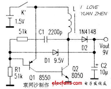
This circuit is easy to start, and the conditions for stable operation without oscillation are:
R1 should be relatively small. After Q1 and Q2 are turned on, C1 completes its reverse charging, and the current through Q1 reaches a minimum. If Q2 remains in saturation (due to the internal resistance of L1 limiting the collector current), the circuit will consume a lot of power and eventually stop operating.
3.7V Boost to 12V Booster Circuit Diagram (2)3.7V to 12V at 1.5A, this is a typical non-synchronous rectification boost circuit. The peripheral components are simple, and an external Schottky diode is used.
Overcurrent protection (OCP) detects the MOSFET current between LX and GND, which corresponds to the peak inductor current. When overcurrent is detected, the duty cycle is reduced, and the inductor current also decreases. If the duty cycle exceeds 50%, OCP further reduces the duty cycle to stabilize the PWM signal. To ensure stable square wave output, the IC internally provides slope compensation. The higher the duty ratio, the lower the OCP threshold. OCP is adjusted using an external resistor R3, with values ranging from 150kΩ to 51kΩ, corresponding to OCP thresholds from 2A to 10A. The OC pin should not be left unconnected.
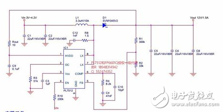
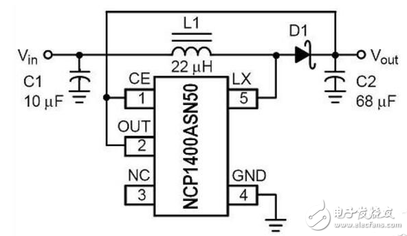
Several IC models are available for 3.7V to 12V boosting, including NCP1400ASN50, NCP1402SN50, CS5171, TPS60110, TPS60111, MAX756, MAX777, MAX731, and MAX770. Among these, the NCP1400ASN50 and NCP1402SN50 are more cost-effective, with retail prices around 2 yuan. They support input voltages from 0.8V to 5V. On the other hand, the TPS60110 and TPS60111 have a simpler design, requiring only 3–4 small capacitors and no switching diodes or inductors. Their input voltage range is 2.7V to 5.4V.
Function description
The socket is ordinary converter,with two output 5V2A power USB power supply at the same time,can be very convenient in use electrical appliances and recharge the equipment at the same time,such as digital products like Iphone Ipad,MP3,MP4 etc.The charge apply to full range of international AC output,no-load power consumption less than 0.3W,with short circuit,overload,over-voltage protection,can be convenient for your life and save more energy
Timer Control Time Adgustment
1.Press the power switch 1 time,the 1HOUR LED will light on.The Timer into ON mode,USB and control socket output ON .
2.Continuously press the power switch the LED light on,the Countdown mode and LED light on will cycle change from 1HR,2HR,4HR,6HR,8HR,10HR.
3.Choose you need countdown time mode,the mode LED will lighto on,start countdown until countdown time finish,the control output and USB change to OFF
4.Then the countdown is start,The Time indicate LED will from high to low auto change until Countdown finish off.
Failure analysis:
1.check whether the power supply connection is good
2.check whether the USB cable is loosen
Warning Note:
1.Use indoor and dry location ONLY
2.The load max does not exceed 15A 3600W
3.This product does not convert voltage please do not miss use DO NOT exceed the maximum loading of 3600 Watts 15A
4.Always have earth connection for safety reason
5.If in doubt please consult with a qualified electrician
USB Countdown Timer, USB Countdown Timer Socket, USB Timer, USB Charger Timer, USB Timer Socket
NINGBO COWELL ELECTRONICS & TECHNOLOGY CO., LTD , https://www.cowellsockets.com