Gallium (Ga) is a chemical element with an atomic number of 31. Unlike many elements, gallium does not occur naturally in its pure form but is typically found as a by-product of the production of zinc and aluminum. This unique property makes it an important material in various industrial applications.
The GaN compound consists of one gallium atom and one nitrogen atom, forming a crystal structure known as wurtzite, which is the most common form. The wurtzite structure is hexagonal and is defined by two lattice constants, usually denoted as 'a' and 'c'. This structural characteristic plays a crucial role in determining the physical and electrical properties of GaN.
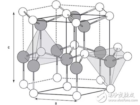
**GaN Crystal Structure**
In the semiconductor industry, GaN is commonly grown using techniques such as metal organic chemical vapor deposition (MOCVD) or molecular beam epitaxy (MBE). These processes are carried out on heterogeneous substrates, such as silicon carbide (SiC) for radio frequency (RF) applications and silicon (Si) for power electronics. The growth occurs at high temperatures, around 1,100°C, ensuring the formation of high-quality GaN layers.
GaN-on-SiC is particularly advantageous for RF applications because it combines the high power density of GaN with the excellent thermal conductivity and low RF loss characteristics of SiC. This makes it ideal for high-power, high-frequency systems like radar, base transceiver stations (BTS), satellite communications, and electronic warfare. Today, GaN-on-SiC substrates can be as large as 6 inches in diameter.
On the other hand, GaN-on-Si offers a more cost-effective solution, though it has lower thermal performance and higher RF losses compared to GaN-on-SiC. Despite these limitations, it remains a popular choice for price-sensitive power electronics applications. The availability of larger substrates—up to 12 inches in diameter—further enhances its appeal in mass production.
So why is GaN considered superior in RF applications? Compared to traditional semiconductors like silicon (Si) and gallium arsenide (GaAs), GaN is a relatively newer technology. However, it has quickly become the preferred choice for high-RF, high-power applications, such as long-range communication systems and high-power transmitters.
**GaN-on-SiC stands out in RF applications for the following reasons:**
**High Breakdown Electric Field:** GaN has a wide bandgap, allowing it to withstand much higher electric fields than other semiconductors. This leads to higher operating voltages, enabling GaN devices to handle more power without breaking down. The ability to operate at higher voltages makes GaN ideal for high-power RF systems.
**High Saturation Velocity:** Electrons in GaN can reach very high velocities under strong electric fields. When combined with high charge carrier density, this results in significantly higher current densities. Since RF power output depends on both voltage and current, GaN devices can deliver much greater power per unit area.
**Excellent Thermal Properties:** GaN-on-SiC benefits from the high thermal conductivity of SiC, which helps dissipate heat more efficiently. This means that GaN-on-SiC devices remain cooler under the same power conditions compared to GaAs or Si-based devices. Lower operating temperatures improve device reliability and longevity.
Overall, GaN’s combination of high breakdown voltage, fast electron mobility, and superior thermal management makes it a game-changer in the world of RF and power electronics. Its advantages continue to drive innovation across a wide range of applications.
Home energy storage system,reliable house generators,hybrid solar system,home backup power,whole home solar system,small solar system for home,house backup battery
EMoreShare International Trade (Suzhou) Co., Ltd , https://www.emoreshare.com