In the DAC Fundamentals: Static Specifications, we explored static specifications and their effects on DC offset, gain, and linearity. These characteristics are basically consistent across the various topologies of the balanced dual resistor (R-2R) and the resistor string digital-to-analog converter (DAC). However, the performance of the short-term glitch interference of the R-2R and the resistor string DAC is significantly different.
We can observe that the dynamics are not linear when the DAC is operating at the working sample rate. There are many reasons for dynamic nonlinearity, but the most influential are short-term glitch interference, slew rate/stability time, and sample jitter.
The user can observe short-term glitch interference while the DAC is operating at its stable output rate over its output range. Figure 1 shows a 16-bit R-2R DAC, such a phenomenon on the DAC8881.
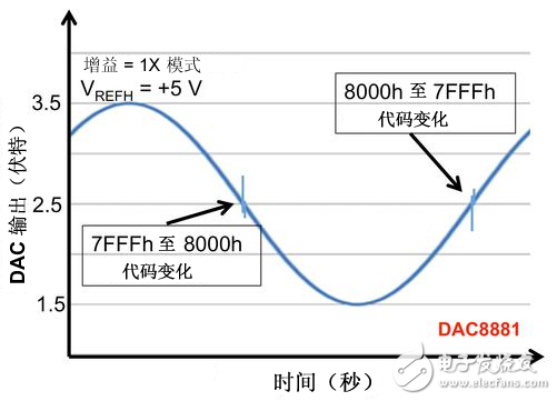
figure 1
This 16-bit DAC (R-2R) output shows the characteristics of short-term glitch interference when the 7FFFh – 8000h code changes.
In the end what happened?
Ideally, the output of the DAC moves from one voltage value to the next in the expected direction. But in reality, the DAC circuit has undershoot or overshoot characteristics during some code-to-code conversion.
This feature is inconsistent every time code to code conversion. The undershoot or overshoot characteristics produced by some conversions are more pronounced than others. These characteristics are quantified by the short-term glitch interference specification. The DAC short-term glitch interference instantaneously outputs an erroneous voltage to interfere with the closed-loop system.
Figure 2 shows an example of a DAC with single-shot short-term glitch interference. A resistor string DAC typically produces this type of short-term glitch interference.
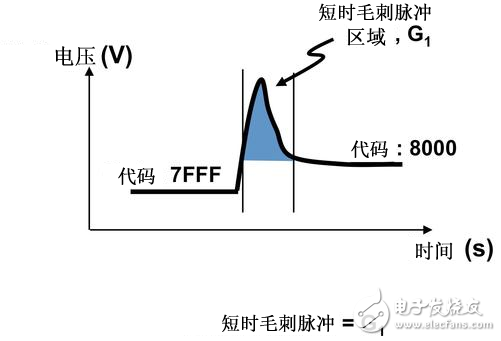
figure 2
The single-shot DAC outputs short-term glitch interference characteristics.
In Figure 2, the location of the transcoding is from 7FFFh to 8000h. If you convert these numbers to binary form, you need to be aware that each bit of the two hex codes is either converted from 1 to 0, or from 0 to 1.
The short-term glitch interference specification quantifies the energy of this glitch phenomenon, in nanovolt seconds, or nV-sec (GI). The number of short-term glitch impulses is equal to the area under the curve.
Single-shot short-term glitch interference is caused by the out-of-synchronization of the DAC's internal switches. What caused this DAC phenomenon? The reason is that the synchronization of the internal DAC switch is not always accurate. You can see these charge exchanges on the output of the DAC due to the charging or discharging of the integrated switched capacitor.
The R-2R DAC produces short-term glitch interference errors in two regions (Figure 3). Due to the double pulse error, the short-term glitch interference (G2) is subtracted from the negative short-term glitch interference (G1) to produce the final short-term glitch interference specification.
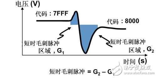
image 3
DAC with R-2R internal structure exhibits double burst short-term glitch interference
The code conversion in Figure 3 is still from 7FFFh to 8000h.
In order to understand the source of DAC short-term glitch interference, we must first define the main carry conversion. At the main carry transition point, when the most significant bit (MSB) goes from low to high, the lower bit goes from high to low, and vice versa. One such code transformation example is 0111b to 1000b, or a more obvious change from 1000 000b to 0111 1111b.
Some people may think that this phenomenon occurs when the output of the DAC exhibits a large voltage change. In fact, this is not the case with every DAC encoding mechanism. See Reference 1 for more details.
Figures 4 and 5 show the effect of this type of glitch pulse on an 8-bit DAC. For DAC users, this phenomenon occurs in a single least significant bit (LSB) step, or in a 5V, 8-bit system at 19.5mV steps.
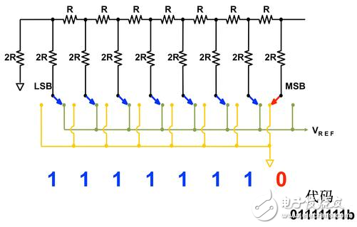
Figure 4
In this 8-bit DAC configuration, this internal switch has seven R-2R pins connected to VREF and one R-2R pin to ground.
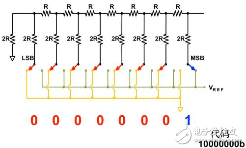
Figure 5
In this DAC configuration, this internal switch has one R-2R pin tied to VREF and seven R-2R pins grounded.
When the DAC loads the code, there are two areas that produce an output glitch pulse: simultaneously triggering the switch synchronization and switching charge transfer of multiple switches.
This resistor string DAC has a single switching topology. A resistor string DAC tap is connected to a different point of the giant resistor string. The switching network does not require multiple conversions on the main carry, so the likelihood of generating a glitch pulse is low. The switching charge will produce a smaller glitch pulse, but it is insignificant compared to the glitch pulse produced by the R-2R structure DAC.
During code conversion, the R-2R DAC has multiple simultaneous switching. Any lack of synchronization causes the short-term switches to be all high or all low, causing the voltage output of the DAC to migrate to the voltage rail. These switches then recover, producing a single-shot short-term glitch interference in the opposite direction. Then the output is stable.
The voltage position of these glitch pulses is fully predictable. In the worst case when using the R-2R DAC, the glitch error occurs when all digital bits are switched while still being converted with small voltage changes. In this case, the DAC code change is performed with the main carry conversion; from code 1000... to 0111....
Hospital Bed Lift,Medical Bed Lift,Hospital Hoyer Lift,Hospital Lifts For Patients
XI'AN TYPICAL ELEVATOR CO., LTD , https://www.chinaxiantypical.com