0 Preface
Handheld multimedia terminals have attracted much attention for their high-permeability mobile digital media, new business concepts and huge market potential, and have become an important area for active research and development of the broadcasting and telecommunications industries in the world. Handheld multimedia terminals have the advantages of high integration, low power consumption and flexible use, so they can be widely used in various fields. The design of human-machine interface for handheld multimedia terminals is becoming more and more human and diversified. The OMAP5912 microprocessor is used in this system. In addition to its low power consumption and high performance, its rich outer ring interface provides support for various human-machine interfaces and is one of its important factors.
1 LCD display design
1.1 interface framework
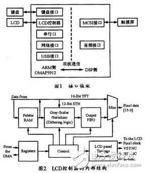
The human-machine interface included in the design of the terminal is a keyboard, a touch screen and an LCD display, and FIG. 1 is an interface structure frame thereof. The function modules are described separately in the following sections.
1.2 LCD controller
The internal structure of the LCD controller in this design is shown in Figure 2. In the figure, the VSYNC signal is a vertical sync signal (also called a frame sync signal) for indicating the start of a new one frame image; the HSYNC signal is a horizontal sync signal (or a line sync signal) for giving a new line of scan signals. The beginning: Ac-bias is the enable signal. The number of dots and the number of rows in each row of the controller are programmable and can be controlled by the registers TIming 0 and TIming 1, respectively. The TFT used in this system is Samsung's LTV350QV_FOE, which uses 320 & TImes; 240 pixel LCD output.
1.3 LCD driver implementation
The frame buffer device is a character device, and its purpose is to establish an automatic transmission channel between the defined memory and the LCD through the configuration register. In this way, any program can change the display content on the LCD by modifying the data in the memory. The frame buffer device driver also adopts the "file layer-drive layer" interface mode.
The most important structure driven by the framebuffer is fb_info, which records the frame buffer device, that is, all the information of the current graphics card, including the parameters, status, and operation function pointers of the device. Each frame buffer device must correspond to one such structure.
The device file corresponding to the frame buffer device is /dev/fb*. If the system has multiple graphics cards, Linux can also support multiple frame buffer devices, up to 32, which are /dev/fb0 to /dev/fb31, and /dev/fb is the current default frame buffer device. Usually points to /dev/fb0. Of course, in an embedded system, it is usually sufficient to support one display device. The frame buffer device is a standard character device. The major device number is 29, and the minor device number is 0 to 31, which corresponds to /dev/fb0 to /dev/fb31. Therefore, the display module loading process usually involves the following steps:
(1) assigning a dma address;
(2) initializing the structure;
(3) Initialize the hardware and configure the corresponding registers;
(4) The application is interrupted;
(5) Register the frame buffer device.
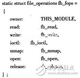
At the file level, Linux defines read operations, write operations, mapping operations, open operations, and shutdown operations. The definition code is as follows:
The open() and release() operations in the file_operaTIons structure do not require underlying support, and the read and write interfaces are no different from ordinary character drivers, except that the object being read and written becomes a framebuffer. It is a pure memory operation. Since Linux works in protected mode, each application has its own virtual address space, and the physical buffer address cannot be directly accessed in the application. For this reason, linux provides the mmap function in the file operation file_operations structure, usually The contents of the file are mapped to user space. For the frame buffer device, the physical address of the screen buffer can be mapped to a virtual address in the user space through a mapping operation, after which the user can access the screen buffer by reading and writing the virtual address. In fact, applications that use framebuffer devices display graphics through mapping operations.
2 touch screen input design
2.1 touch screen chip ADS7843
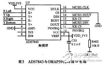
ADS7843 is a four-wire resistive touch screen conversion interface chip produced by TI. It is a 12-bit sampling analog-to-digital converter with a synchronous serial interface. Pins X+, Y+, X-, Y- are the analog inputs of the converter; DCLK is the external clock input; CS is the chip select; DIN is the serial input, control data can be input through this pin; DOUT is serial Data output, can be used to output the converted touch position data; IN3, IN4 are auxiliary inputs; PENIRQ is the PEN interrupt pin.
This design mainly realizes serial input and output of commands and data with ADS7843 through MCSI interface, and is multiplexed into GPIO through KB.C pin, and then realizes interrupt trigger of PENIRQ and BUSY signals. Figure 3 shows the interface circuit diagram of the ADS7843 connected to the OMAP5912.
2.2 touch screen driver
Since the design is to send commands and read touch screen data by the MCSI interface on the DSP side, and the data is transmitted to the interface program by the operating system on the ARM side, the driver uses the MAILBOX dual-core communication to implement the intermediate transfer.
The processing flow on the ARM side is as follows:
(1) MAILBOX interrupt on the ARM side;
(2) The X, Y is read from the data register DSP2ARM and the command register DSP2ARM2B by the MAILBOX interrupt service program, and is packaged into a touch screen return structure TS_RET, and finally written to the queue through the write pointer;
(3) The data is read by the application through the read pointer and processed accordingly.
There are two important structures in the driver:

3 keyboard input design
The OMAP5912 supports keyboard-specific 8×8 I/O interfaces as well as KB.R[7:0] and KB.C[7:0]. KBR_LATCH is the keyboard row input, and KBC_REG is the keyboard column output. By reading and writing these two registers, the row and column can be scanned. In order to save system resources and improve the efficiency of use, this design uses a combination of interrupt and scanning to implement 3×3 keyboard driver.
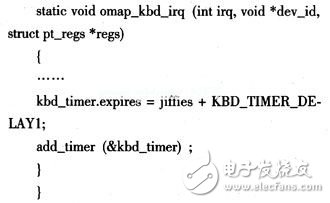
When the key interrupt is generated, in order to eliminate the jitter, the key value is not determined first, but the timer is started, and the key value is read in the timer interrupt. The process of reading the key value is to first determine the row line, and then determine the button value by the column scan code.
The keyboard interrupt service routine is given below:
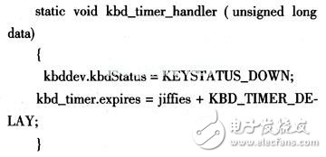
The timer interrupt service routine is as follows:
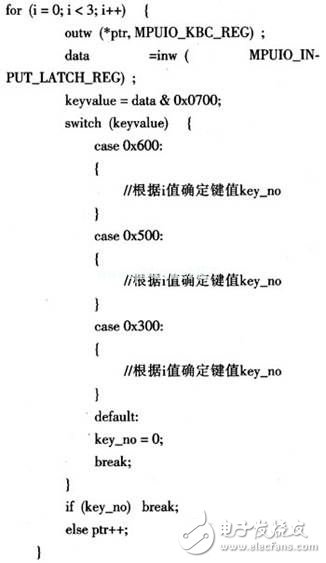
Here is the scanner:
4 Conclusion
This paper introduces the driver development method of the human-machine interface under the OMAP5912 platform. The completed driver can run normally under the Montavista Linux operating system, which is instructive for the development of drivers for other devices under this platform. The OMAP open multimedia application platform also reserves enough space for the future expansion of the system. It is believed that the system will have great market potential.
Guangzhou Ehang Electronic Co., Ltd. , https://www.ehangmobile.com