Gallium (Ga) is a chemical element with an atomic number of 31. Unlike many elements, gallium does not occur naturally in its pure form but is typically found as a by-product during the production of zinc and aluminum. This unique property makes it essential to understand how gallium is sourced and processed for industrial applications.
The GaN compound consists of one gallium atom and one nitrogen atom, and it most commonly adopts a wurtzite crystal structure. The wurtzite structure is hexagonal in nature and is defined by two lattice constants, usually denoted as 'a' and 'c'. This structural characteristic plays a crucial role in determining the material's physical and electronic properties.
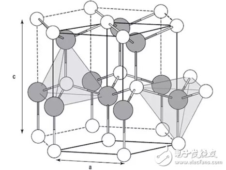
As shown in the image above, the GaN crystal structure provides the foundation for its use in advanced semiconductor technologies. In the semiconductor industry, GaN is typically grown using techniques such as metal organic chemical vapor deposition (MOCVD) or molecular beam epitaxy (MBE), often on heterogeneous substrates like silicon carbide (SiC) or silicon (Si). These processes take place at high temperatures, around 1,100°C, ensuring the formation of high-quality crystalline layers.
GaN-on-SiC is particularly advantageous for RF (radio frequency) applications due to the combination of GaN’s high power density and SiC’s excellent thermal conductivity and low RF loss. This makes GaN-on-SiC ideal for high-power, high-frequency systems such as radar, base transceiver stations, satellite communications, and electronic warfare. Today, GaN-on-SiC substrates are available in sizes up to 6 inches in diameter.
On the other hand, GaN-on-Si offers a more cost-effective solution for power electronics applications. While its thermal performance and RF efficiency are lower compared to GaN-on-SiC, the reduced cost makes it a popular choice for price-sensitive markets. Current GaN-on-Si substrates can be as large as 12 inches in diameter, supporting broader adoption in various industries.
So why is GaN considered superior for RF applications? Compared to traditional semiconductors like silicon (Si) and gallium arsenide (GaAs), GaN is relatively new but has quickly become the preferred choice for high-power and high-frequency applications. Its ability to handle long-distance signals and high power levels makes it ideal for demanding environments.
GaN-on-SiC stands out in RF applications for several key reasons:
**High Breakdown Electric Field:** GaN has a wide bandgap, allowing it to withstand much higher electric fields than other materials. This leads to higher operating voltages, enabling GaN devices to support more powerful applications without degradation.
**High Saturation Speed:** Electrons in GaN move at very high speeds under strong electric fields. Combined with GaN’s high charge capacity, this allows for significantly higher current densities, resulting in greater RF power output.
**Excellent Thermal Properties:** GaN-on-SiC benefits from the high thermal conductivity of SiC, which helps dissipate heat more efficiently. As a result, these devices operate at lower temperatures, improving reliability and longevity compared to GaAs or Si-based devices.
Overall, GaN’s unique combination of electrical, thermal, and mechanical properties makes it a game-changer in modern electronics, especially in RF and power applications.
Solar Home System,Solar System,Household Energy Storage System,Home Standby Generator
EMoreShare International Trade (Suzhou) Co., Ltd , https://www.emoreshare.com