1. Introduction
With the rapid advancement of information technology, the real-time collection and processing of various data have become essential in modern industrial control and scientific research, particularly in high-speed and high-precision signal measurement, image processing, and audio signal analysis. To meet these demands, high-performance data acquisition techniques are crucial. This leads to two key requirements for data acquisition systems: first, the interface must be simple, flexible, and capable of high-speed data transfer; second, due to the large volume of data, the host system needs to respond quickly, enabling real-time analysis and processing. In software-defined radio (SDR) receiver architectures, digital down conversion (DDC) plays a central role and is considered one of the core technologies. After analog-to-digital conversion (ADC), DDC processes high-speed and high-capacity data, making it challenging to implement. To address these challenges and the specific requirements of data acquisition systems, this report presents a high-speed data acquisition and real-time transmission solution based on FPGA and USB 2.0 technology. The system discussed in this paper utilizes a Spartan-6-based architecture to achieve high-speed orthogonal IQ data output from a broadband IF digital receiver to the FPGA, enabling subsequent signal processing in software-defined radio applications. The Cypress EZ-USB FX2 is used for high-speed data transmission of baseband signals or data processed by the FPGA, while host computer software handles storage and display. This paper covers three main aspects: the high-speed data acquisition module (wideband IF digital down-conversion), the high-speed data transmission module, and the host computer software, with an emphasis on both hardware and software design.2. System Overall Design
The entire system is divided into three main sub-modules: (1) the high-speed data acquisition module (wideband IF digital down-conversion module), (2) the high-speed real-time processing and transmission module, and (3) the upper computer software module. The overall system block diagram is shown in Figure 1: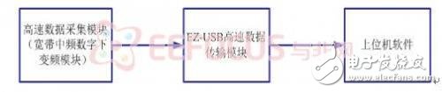
Figure 1: System Overall Principle Block Diagram
The high-speed data acquisition and EZ-USB high-speed transmission modules are composed of corresponding hardware circuits and software. The PC software module is primarily developed using MFC with Microsoft Visual Studio 2008. The overall hardware block diagram is illustrated in Figure 2: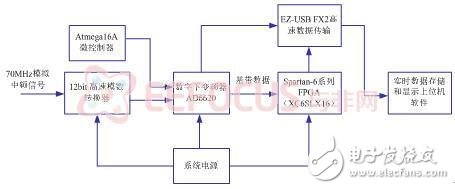
Figure 2: System Hardware Block Diagram
The working principle of the system is as follows: First, the high-speed data acquisition module performs analog-to-digital conversion on a 70MHz IF analog signal at a sampling rate of 60MHz, based on the bandpass sampling theorem. An Atmel Atmega16A microcontroller is used as the control unit for asynchronous control and special digital down-conversion programming, shifting the 70MHz intermediate frequency signal to the digital baseband. The baseband data rate remains at 60MHz, so high-speed digital baseband signals need to be extracted and filtered to obtain low-speed baseband signals. The extraction ratio can be programmed, with smaller factors resulting in lower baseband signal rates. The low-speed baseband data is then sent to the FPGA for symbol recovery, extracting the original information. The EZ-USB FX2 facilitates real-time data acquisition and transmission of the digital baseband signal and the symbol information generated by the FPGA. Finally, the data is transferred to the host computer via the USB 2.0 interface for real-time storage and visualization.3. High-Speed Data Acquisition Module (Wideband IF Digital Down Conversion Module)
Traditional data acquisition systems often use microcontrollers or digital signal processors (DSPs) to control ADCs, memory, and other peripherals. However, due to the limitations of MCU clock speed and instruction cycle, all functions are implemented through software, which consumes significant time during the sampling process, reducing efficiency and making it difficult to meet real-time and synchronization requirements. Although DSP-based systems offer faster processing speeds, they come with higher costs and frequent interruptions that can degrade CPU performance and response times. In recent years, FPGA-based data acquisition solutions have gained popularity due to their unique advantages. One of the most important benefits is the ability to perform parallel data processing. Additionally, FPGAs offer a short development cycle, high integration, low power consumption, high operating frequency, and flexible programming, making them ideal for high-speed and complex data acquisition tasks. The high-speed data acquisition and real-time transmission scheme presented in this report includes three key components: high-speed data acquisition and digital down-conversion processing, high-speed data transmission, and the upper computer data acquisition control section. The system first digitizes the external analog signal, buffers the high-speed digital output from the ADC, transfers the buffered data to the FPGA after digital down-conversion, and uses the FPGA to control the CY7C68013A chip for high-speed real-time data transmission, storage, and display.Solar tracker system,Fully automatic solar tracker,Solar tracker structure,Solar tracker bracket
Hebei Shuobiao New Energy Technology Co., Ltd. , https://www.pvbracketsystem.com