introduction
This article refers to the address: http://
With the development of society, urban public transportation has become an indispensable part of our lives. At present, bus fares mainly include manual ticketing and credit card charging. Although manual ticketing has the advantage of being supervised and effective in preventing the phenomenon of ticket smuggling, it is necessary to pay wages to the ticket seller every month, thereby increasing the cost. Cards and coin-operated charges can solve the cost problem, but it is very inconvenient for passengers to get on and off the bus, especially during peak hours, which greatly slows down the speed of getting on and off. At present, the operating distance between the RF card and the toll collection machine used for bus fares at home and abroad does not exceed 0.1 m (hereinafter referred to as the “near cardâ€), the passengers need to take the card from the pocket, take the card, and close the toll machine to swipe the card. Putting the card back into the pocket and the bag, these actions slow down the speed of the passengers on board, especially for passengers carrying things with their hands, the card swiping operation is very inconvenient.
The bus automatic toll collection system studied in this paper uses active tags to complete the design of the bus card. On the basis of ensuring a long service life, the sensing distance is increased to about 1 m. The vehicle system is placed at a distance of about 1 m from the door of the bus. When the passenger gets on the bus, the vehicle system can successfully swipe the card. At the same time, the anti-collision algorithm is used to ensure that the passenger can successfully swipe the card when the passenger is crowded. Low cost and high efficiency. In recent years, the vigorous development of subway transportation has brought great convenience to people's travel. The system can also be used for automatic toll collection of subways after modification, and the application space is relatively wide.
1 The overall composition of the system
The bus far-card automatic toll collection system is divided into two parts: the bus card and the vehicle system. The bus card is mainly composed of nRF24LEl RF module and wake-up circuit; the vehicle system is mainly composed of main processor STM32, GPS positioning module, liquid crystal display circuit, storage circuit, voice report station circuit, wake-up circuit and so on. The overall structure of the system is shown in Figure 1.
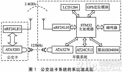
When the passenger carries the bus card and passes the vehicle system, the ATA5283 wake-up circuit of the bus card receives the 125 kHz electromagnetic wave sent by the ATA5276 chip of the in-vehicle system reader, activates the bus card in the sleep mode, and the bus card enters the transmission mode. Send your ID number and card amount to the in-vehicle system. The in-vehicle system sends a message to the bus card, and the buzzer sounds to indicate that the card is successfully swiped, and the success message is displayed on the LCD screen. At the same time, the in-vehicle system saves the ID number, amount, and boarding position of the bus card in the AT24C512 memory. When the passenger wants to get off the bus and approaches the card reader again, the bus card is woken up again and sends data to the in-vehicle system. The processor of the vehicle system finds the amount of the deduction required according to the ID number of the bus card to calculate the amount of the deduction required, and sends the deduction data to the bus card; at the same time, the ride information is saved in the database. For use in the query. After the bus arrives at the terminal, it will be reset. If there is a passenger who fails to sense when getting off the bus, the deduction will be made according to the distance to the terminal.
2 main part of the system hardware implementation
2.1 The hardware design of the bus card
Using nRF24LE1 as the tag chip, ATA5283 is used as the wake-up chip to form the hardware circuit of the bus card. nRF24LE1 is a 2.4 GHz transceiver chip with processor. It integrates 51 core and nRF24L0 1 transceiver core on a small chip. It uses the same embedded protocol and GFSK modulation method as nRF24L01. It has serial port, SPI and I2C. Rich in peripheral resources such as PWM generators and random function generators, the chip consumes very low power and has non-volatile data memory.
The ATA5283 is a 125kHz wireless wake-up chip with high detection sensitivity and ultra-low power consumption. It has a sensitivity of 1 mV and consumes only 1~2μA when listening to the 125kHz data state. In the process of receiving 125 kHz data, The power consumption is 2 to 4 μA. When receiving 125 kHz data, at least a 125 kHz carrier duration of 5.64 ms is detected before entering normal operating mode. The time of the first 1.54 ms carrier period is used to wake up the chip, and the last 4.1 ms carrier period is used for self-gain adjustment to adjust the amplification gain of the received signal to an appropriate value. The peripheral circuit, such as the button battery, constitutes an active bus card, enabling long-distance signal transmission and reception. The bus card hardware circuit is shown in Figure 2.
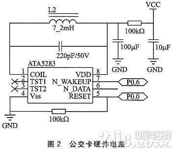
When no 125 kHz signal is detected, the ATA5283 chip is in standby mode with very low power consumption. In this mode, the antenna end of the COIL pin is always detecting whether a carrier signal arrives, the N_DATA and N_WAKEUP pins are high, and the reset pin RESET is in a low state. When the antenna end of the COIL pin receives at least 704 carrier sequences, the ATA5283 chip enters the operating mode, N_DATA begins to receive carrier data, and N_WAKEUP goes low, waking up nRF24L E1. Since only the wake-up function is required, no effective carrier data transmission is required, so it is only necessary to connect N_WAKEUP to the P0.6 pin of nRF24LE1. Finally, the P0.0 pin of the nRF24LE1 gives a high level to the RESET pin of the ATA5283, resetting the ATA5283 and returning the chip to standby listening mode.
2.2 Automotive system RF module circuit design
The nRF24L01 RF module is compatible with the RF part of the nRF24LE1. It also operates in the 2.4 GHz frequency range and is a wireless transceiver chip for the general ISM band. Built-in RF transceiver, data buffer, GFSK modulation/demodulator, enhanced mode control unit and SPI interface connected to the processor. The nRF24L01 communicates with the processor using the SPI bus, and the STM32 processor comes with an SPI interface.
The design of the clock control signal SCK, serial data output MISO, serial data input MOSI, chip enable pin CSN, interrupt signal IRQ, RF enable pin CE and processor PA5, PA6, PA7, PC4, The PB0 and PC5 pins are directly connected. The specific circuit is shown in Figure 3. At the same time, the chip's enhanced mode has automatic retransmission and auto-answer function. The interrupt signal IRQ is used to tell the processor the status of receiving and transmitting data, so that the processor can make corresponding processing according to the status in time. These functions are greatly reduced. The workload of the MCU.

2.3 Design of low frequency wake-up transmission circuit for vehicle system
The active tag is activated by continuously transmitting low-frequency 125 kHz electromagnetic waves. The transmitting chip adopts ATA5276, which can transmit a signal with a frequency of 125 kHz. The peak current of the chip driving the antenna coil is adjustable, and the maximum peak current of the output can reach 1.5. A, the modulation mode is ASK modulation, the baud rate can reach 4Kps, and the working voltage range of the chip is 8~24V. When in standby mode, the current consumption is less than 50 μA, and the transmitted 125 kHz electromagnetic wave is transmitted to the corresponding receiver. The chip can be controlled by the PD0 pin of STM32.
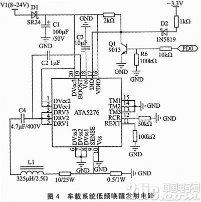
Set the DIO pin to the 唧 pin of STM32. As shown in Figure 4, the PD0 pin is normally in a low state. When PD0 is high, the transistor is turned on, the DIO pin goes low, and the ATA 5276 is The standby mode is changed to the working transmission mode; at this time, DIO is low level, the series resonant circuit composed of L1 and C4 starts to start, and 125 kHz energy propagates through the inductor as a magnetic field, when the DIO pin detects low level. Stop the resonance.
3 system software implementation
The software design mainly includes in-vehicle system program design and bus card program design. The in-vehicle system program includes I2C bus program of 舡24C512 memory, serial communication program of GPS, SPI bus program of nRF24L01 and ISD4004, and parallel port programming of CD 12864. The bus card program mainly includes nRF24LE1 low power consumption and anti-collision program design. The programming language is C language, which is flexible and convenient. The software development platform is MDK, which has high integration, online simulation and debugging functions, and is very suitable for embedded development.
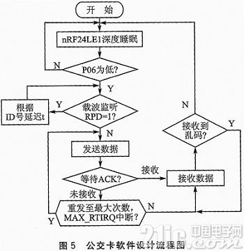
3.1 Bus card software design
The bus card software is designed to ensure that the tag information is sent out accurately and in a timely manner, and the data processed by the card reader is received in time. It mainly consists of three parts: label transmission and reception, low power design, and anti-collision algorithm design. The software flow is shown in Figure 5.
3.2 In-vehicle system RF module software design
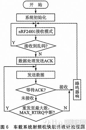
The function of the RF module nRF24L01 of the in-vehicle system is to receive the data information of the card and hand it to the processor for processing. The STM32 communication uses the SPI bus protocol, the STM32 has an SPI port, and is developed using the STM32 library function, which greatly simplifies the programming. As long as the interface function is configured accordingly, the SPI register can be operated. The nRF24L01 has a variety of operating modes. This design uses basic transmit and receive modes. In order to implement automatic response, automatic processing of headers and CRC, the Enhanced ShockBurstTM enhanced mode simplifies programming and reduces the number of operating modes. The burden on the processor, and the ability to receive and send data more timely and accurate. The software implementation process is shown in Figure 6.
Conclusion
The in-vehicle system of this design needs to provide an inductive device at each of the front door and the rear door, requiring the passenger to get on the front door and the rear door to get off. When the current door reader detects that the passenger gets on the bus, the bus card sends the information to the in-vehicle system, and the in-vehicle system responds and records the information sent by the bus card. When the vehicle is running, the wake-up signal of 125 kHz is not sent, so the bus card cannot be woken up, and can only be woken up when the door is opened and the passenger approaches the card reader. When the passenger gets off the vehicle and is detected by the back door sensor, the received bus card information is compared with the last detected information, and the corresponding deduction processing is performed. The simulation program is designed every 1 minute, and the number of stations is increased by 1, indicating that the bus has gone one station, and the deduction standard is 1 yuan per 10 stations. Tested with 10 bus cards. The test results show that the system can complete the data reading and data processing of the card in time.
- STM32 microcontroller Chinese official website
- STM32 microcontroller official development tools
- STM32 microcontroller reference design
| About Glass Fiber Film Covered Flat Copper Wire |
Golden coloured glass fiber insulation ,fiber glass covered enameled film flat wire
Packaging Details : Different size bobbin with export carton/wooden box on pallet , or as customer's requirement.
The product is the premium copper or aluminum to be enameled, then to be wrapped with polyester film or polyimide film so as to enhance the breakdown voltage of enameled wire. It has the advantages of thin insulation thickness, high voltage resistance. The product is the ideal material for electrical instruments of small size, large power, high reliability.

Copper or Aluminum rectangular Wire
Narrow side size a : 0.80mm-5.60mm
Broad side size b : 2.00mm-16.00mm
Copper or Aluminum Round Wire
Diameter:φ1.7-φ5.0
If specification is out of range, please
Glass Fiber Film Covered Flat Copper Wire
Film Covered Copper Flat Wire,Glass Fiber Film Covered Flat Copper Wire,Single Fiber Glass Copper Flat Wire,Fiber Glass And Film Copper Wire
HENAN HUAYANG ELECTRICAL TECHNOLOGY GROUP CO.,LTD , https://www.huaonwire.com