In this paper, a video processing system is designed using TI's TMS320DM642 (hereinafter referred to as DM642) digital multimedia processing chip. The article mainly introduces the hardware design and debugging process of the system.
1 System hardware design
1.1 The hardware structure of the system
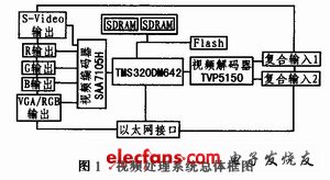
The DSP used in the hardware design of the video processing system is DM642. It is a high-performance digital multimedia processor with a maximum operation speed of 5760 MIPS (million instructions per second), which can meet the real-time processing requirements of complex algorithms. The video signal needs to be collected by the CCD camera.
The video decoding chip converts the collected analog signals into digital signals for DSP to perform arithmetic processing. There are 3 video interfaces (VP ​​ports) of DM642, among which VP0 and VP1 are 20 bits, 10 bits are used for video input, and the other 10 bits are used for audio input. The VP2 port is also 20 bits and can be divided into two video inputs. In the video processing system designed in this paper, the analog video signal collected after the analog-to-digital conversion of the video decoding chip forms a digital video signal in BT.656 format, which is input through the VP0 port of DM642.
The digital signal is encoded and compressed by the software encoder of DM642, and the video stream data generated by the encoding and compression is packaged and transmitted to the remote upper computer via the RJ-45 interface via Ethernet. The upper computer acts as a server, thus forming a monitoring system. Through the DM642 independent multimedia interface (MII), an Ethernet processing chip is connected outside the chip to form a 10/100 Mbpa Ethernet module. Local playback is done by the video encoding chip.
SDRAM and Flash memory can be connected through the EMI642 interface of DM642. Although DSP provides on-chip RAM, in most cases it cannot meet the requirements of the system; at the same time, for systems that require real-time processing, it is also necessary to minimize the time overhead caused by memory read and write during data flow, so High-performance SDRAM is configured in the system, which is used when running programs and data processing. Flash is mainly used to store system software and configuration parameters in the system.
The overall block diagram of the system is shown in Figure 1.
A considerable number of on-board devices are integrated on the video processing system to adapt to different application environments. Its main features are:
1) The operating frequency of the system is 600 MHzc.
2) 2 video ports: 1 for on-board decoder and 1 for on-board encoder.
3) 32 MB of synchronous DRAM space.
4) 2 MB of Flash space.
5) Ethernet interface.
6) Equipped with emulator interface can be used for JTAG emulation.
7) The supply voltage is +5 V.
8) Buzzer alarm.
1.2 Memory module design
In the data processing module, the three chips of DSP chip, SDRAM chip and Flash chip are the core of the entire module circuit. The function of this module is to complete the data transmission with the external data storage and the program read and write tasks of the program storage. Connected to the emulator through the JTAG interface circuit and connected to the computer host for simulation and debugging, to achieve data exchange with the target host.
1.2.1 SDRAM interface design
In the hardware design of the system, the SDRAM memory chip uses MT48LCAM3282-1Mx32 & TImes; 4 banks produced by Micron. SDRAM, or Synchronous DRAM (Synchronous Dynamic Random Access Memory), indicates that its working speed is synchronized with the bus speed of the system. The highest clock of MT48LC4M3282 bus is 166 MHz. It is mainly used to store data and programs. The refresh of SDRAM is automatically controlled by the DSP chip. MT48LCAM3282 is a high-speed CMOS dynamic random access memory, which is internally configured as a 4-zone synchronous interface.
EMI642 of DM642 can program the address attribute of SDRAM, and it can realize seamless connection with SDRAM. The largest clock bus of EMIFA can reach 133 MHz. The SDRAM controller can support SDRAM chips from 16 M to 256 Mbit. Cache capacity on TMS320DM642 is limited, so video data is usually stored in off-chip SDRAM. When it is needed, the data is moved from off-chip to on-chip processing through EDMA, so that the execution efficiency of the program can be improved. The SDRAM interface diagram of TMS320DM642 is shown in Figure 2.
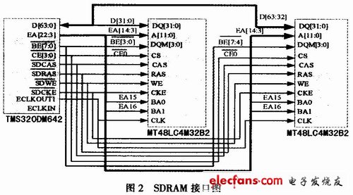
Because the data bus of TMS320DM642 is 64 bits, and the data bus of each MT48LC4M3282 is 32 bits, two MT48LC4M3282 need to be connected in parallel to form a 64-bit data bus, so that it can be connected to the EMW data bus of TMS320DM642. Refer to the SDRAM configuration method in the DM642 data manual. EA15 and EA16 control the SDRAM group, EA3-EA14 controls the row address, EA3-EA11 controls the column address, and the chip select signal is connected to the DM642.
In this way, SDRAM is allocated to the CE0 space.
1.2.2 Flash interface design
The asynchronous interface of DM642 EMIFA provides a configurable memory cycle type for various types of memory and peripherals, including SRAM, EPROM, Flash, etc. In this system, Flash uses SST39VF1601 Flash produced by SST, and the chip select signal DM642 on the pin. When the DSP is powered on, the DSP copies 1 K bytes of data from the external CE1 addressing space to the internal storage space through enhanced direct memory access, and then starts running from the internal storage space 0x0, so the Flash ROM must be configured in The CE1 space of DSP, the corresponding address in DSP memory is 0x90000000-0x90200000.
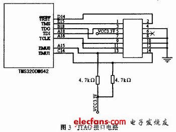
1.3 JTAG interface design
The JTAG interface is the interface between the debugging environment and the target board. Its advantage is that it allows developers to develop the target board without changing the system structure of the target board, thereby facilitating system development and testing. The XDS510 emulator connects the system board to the computer through the JTAG interface, so that you can use the integrated development environment provided by TI to debug the system. The JTAG interface uses a standard dual-row 14-pin socket. The JTAG interface circuit of the system is shown in Figure 3.
Mining Cap Lamps from Win 3 safety are wildely used in construction sites that require a lot of flexibility and mobility, like mining, tunnel projects oil field, it could be also popular in outdoor sports like camping, hiking, diving, caving ,night fishing, night flying, etc.
Win3 team dedicate to provide global mining enterprises with safe& intelligent miner`s lamps and safety solutions. Our products cover Cap Lamps,Miners Lamp,Floodlight/Chargers/Charging system etc. We strive to improve safety and enhance efficiency of global mining and industrial enterprises, sincerely hope that we can build a long standing win-win business relationship with friends overseas.
Cap Lamps,Miners Lamp,Miners Torch,Underground Cap Lamp
ZHEJIANG HUACAI OPTIC-TECHNOLOGY CO LTD , https://www.win3safety.com