For a high-speed serial bus, in general, clock information is embedded into the transmitted data stream by data encoding, and then the clock information is extracted by the clock recovery at the receiving end, and the recovered clock is used to perform data processing. Sampling, so the clock recovery circuit is critical for the transmission and reception of high-speed serial signals.

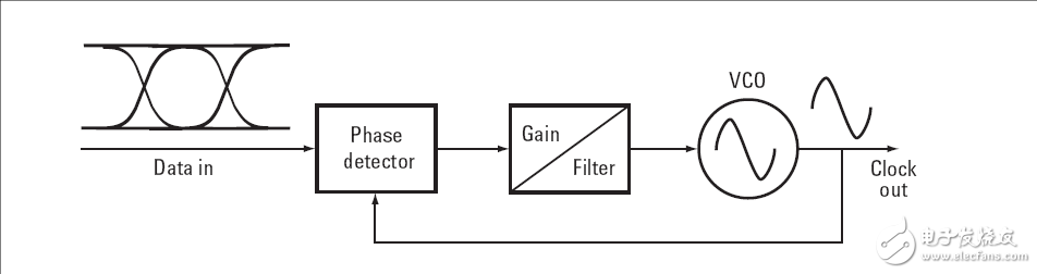
CDR Circuit Principle The purpose of clock recovery is to track the clock drift and a portion of the jitter on the transmit side to ensure proper data sampling. The clock recovery circuit (CDR: Clock Data Recovery) is generally implemented by means of a PLL (Phase lock loop), as shown in the following figure. The input digital signal is compared with the PLL's VCO (Voltage-controlled oscillator). If there is a frequency difference between the data rate and the output frequency of the VCO, a phase difference changes, and the phase detector pairs this phase. The error is compared and converted into a corresponding voltage control signal, and the voltage control signal is filtered by the filter to generate a control signal to the VCO to adjust the output clock frequency of the VCO. The purpose of using the filter is to integrate the fast phase change information into a relatively slow voltage change to adjust the output frequency of the VCO. This filter is sometimes referred to as a loop filter, usually a low pass filter. Through repeated phase discrimination and adjustment, the output signal frequency of the final VCO and the frequency of the input digital signal change, and the PLL circuit enters the locked state.
Effect of Loop Bandwidth on Eye Diagram and Jitter Measurement It is worth noting that in the real world, the input digital signal is not a pure signal, but contains jitter of different frequency components. For low-frequency jitter, it causes a slow change in data rate. If the slowly changing frequency is lower than the bandwidth of the loop filter, the phase change information caused by the jitter of the input signal can be generated by the loop filter. The VCO output frequency is adjusted, and the jitter of the input signal is tracked in the output clock of the VCO. If the frequency of the jitter in the input signal is relatively high, and the phase change signal caused by the signal cannot pass through the loop filter, there will be no jitter component in the clock outputted by the VCO, which is the input signal. The high frequency jitter component is filtered out by the PLL circuit.
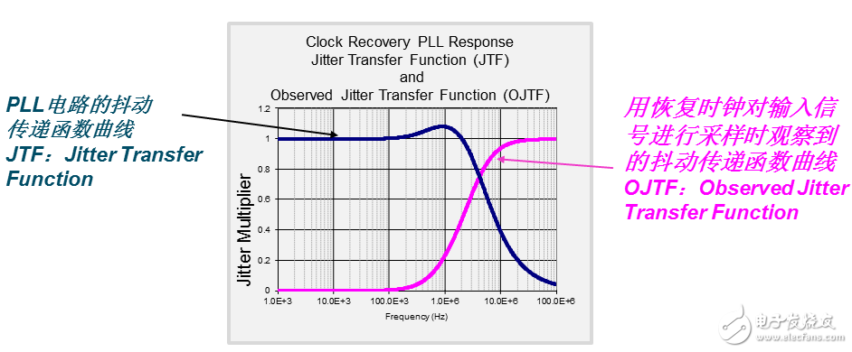
As shown in the figure below, we usually use the JTF (Jitter Transfer FuncTIon) curve of the PLL circuit to describe the transmission capability of the PLL circuit for different frequency jitter. The JTF curve is usually a low-pass characteristic, reflecting the PLL circuit's ability to track well for low-frequency jitter and limited high-frequency jitter tracking.
For low frequency jitter, the PLL circuit is well tracked and the recovered clock is jittered with the signal under test. If the chip at the receiving end samples the input signal based on the recovered clock, since the clock and the signal under test are jittered together, the low-frequency jitter is not observed, and the setup and hold time for the data sampling is not too large. influences.
Conversely, high-frequency jitter is filtered out by the PLL circuit, so the high-frequency jitter components are not included in the output clock. If you use this clock to sample the data signal, you will notice significant jitter in the input signal. The relationship between jitter and jitter frequency that can be seen when the receiver is sampling with the recovered clock is sometimes described by the OJTF (Observed Jitter Transfer FuncTIon) curve. The curve with frequency is just the JTF curve. in contrast.
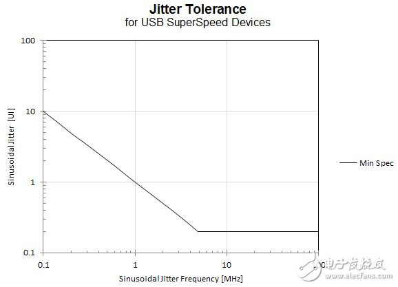
Because of the tracking characteristics of the clock recovery circuit for low-frequency jitter, many high-speed serial bus receiver chips can tolerate low-frequency jitter far beyond the tolerance for high-frequency jitter. The following figure is a curve of the USB3.0 bus for the receiver chip's tolerance for different frequency jitter. It can be seen that its tolerance to low frequencies is very large, and can even exceed one UI (data bit width).
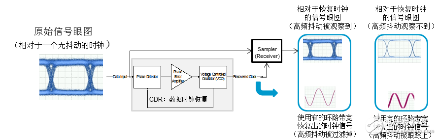
The loop recovery bandwidth of the PLL of the clock recovery circuit is different, and the jitter tracking capability is different for different frequencies. In general, the narrower the bandwidth setting of the PLL, the purer the recovered clock, but the weaker the tracking ability for jitter. The more jitter the signal sees when sampling the data with this clock as the reference, see The worse the eye diagram of the signal will be; on the contrary, if the bandwidth of the PLL is set to be wider, the stronger the tracking ability for jitter, the closer the recovered clock and signal jitter, and the data is sampled when using this clock as a reference. The less jitter on the signal, the better the eye diagram of the signal you see. The figure below shows the different PLL bandwidth settings for recovering clock jitter and the eye pattern seen when sampling the signal based on this recovered clock.
The choice of clock recovery mode in the test As can be seen from the previous introduction, the eye diagram and the jitter are relative quantities. For the same signal, the effect of seeing the clock is different. So what kind of clock should be used as a reference for eye diagram or jitter measurement of a high-speed serial signal? Or what should be the loop bandwidth for clock recovery? The answer is to refer to the clock recovery of the receiving chip as much as possible.
Even for the measurement of the eye pattern and jitter of a signal sent directly from the transmitter, what we care about is what the eye pattern seen after the signal is recovered by the receiving chip after the signal enters the receiving chip, so it is in progress. When the signal quality test at the transmitting end is tested, the clock recovery mode of the receiving end is also simulated as much as possible, otherwise the measured result may be unreal. Different buses have requirements for the loop bandwidth of the receiver clock recovery and even the shape of the filter. For example, 1/1667 or 1/2500 of the data rate in optical communication is used as the loop bandwidth, and PCI-E, USB3.0, Buses such as SATA have their own defined loop bandwidth requirements.
In order to facilitate testing for different buses, the test instrument not only needs to have clock recovery capability, but also needs to be able to set the appropriate loop bandwidth according to the requirements of different buses. Many real-time oscilloscopes use software to perform clock recovery. The loop bandwidth setting is relatively flexible. The sampling oscilloscope or BER tester uses a special hardware clock recovery circuit. In this case, the clock recovery circuit needs to have a ring. The ability to adjust the bandwidth of the road to adapt to different test standards.
Original link: https://
Intermediate Frequency AC Power Supplies
The IFP series is AC Power Supplies with a constant 400Hz output frequency and adjustable output voltage, based on the same technical principle as the adjustable AC power supplies of SPWM method, IGBT module design and D/A conversion technology. The difference is that the output frequency of the Intermediate Frequency AC Power Supplies is constant at 400 Hz, it is a replacement product of unit type variable frequency power supplies with higher output frequency accuracy and stability.

The output power of single-phase Intermediate Frequency AC Power Supplies ranges from 500VA to 200KVA, and the output power of three-phase Intermediate Frequency AC Power Supplies ranges from 3KVA to 600KVA. The output voltage of both types can be divided into 0 ~ 150Vac, 150 ~ 300Vac with 400Hz fixed output frequency. This series of AC power supplies are featured for high precision, stable output, high display resolution, low waveform distortion and complete protection functions.
Through the friendly operation panel, you can read the output data such as output voltage, output current, output power, power factor, etc., providing accurate data records for your test, and can add RS485 interfaces as standard, following the MODBUS-RTU international communication protocol, which can realize remote control and operating status monitoring of the power supplies, Currently, the Intermediate Frequency AC Power Supplies are mainly used for aircraft and mechanical equipment, radar, navigation and other military electronic equipment and other occasions that require 400Hz intermediate frequency output.
Intermediate Frequency AC Power Sources, 400Hz AC Power Supplies, 400Hz AC Power Sources, Middle Frequency AC Power Supplies, AC Power Supplies 400Hz
Yangzhou IdealTek Electronics Co., Ltd. , https://www.idealtekpower.com