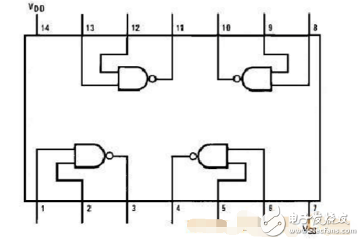
**CD4011 Working Principle and Pin Diagram**
The CD4011 is a CMOS integrated circuit that contains four independent NAND gates. It operates with a power supply of +5V to +15V, typically using pin 14 as the positive supply (VDD) and pin 7 as ground (VSS). Each pair of pins forms a NAND gate: pins 1 & 2 are inputs for one gate, and pin 3 is its output. When both inputs (pins 1 and 2) are high, the output (pin 3) goes low. If either input is low, the output remains high. The other three NAND gates can be used as inverters by connecting their inputs together.
Pin 1 is used for external light control, while pin 2 serves as a trigger delay input. This configuration allows the CD4011 to function in various logic circuits, including flip-flops and oscillators.
**CD4011 Pin Diagram and Function:**
- **1A, 2A, 3A, 4A**: Input pins for the first to fourth NAND gates
- **1B, 2B, 3B, 4B**: Second input pins for each gate
- **1Y, 2Y, 3Y, 4Y**: Output pins for each gate
- **VDD**: Positive power supply (pin 14)
- **VSS**: Ground (pin 7)
**CD4011 Internal Block Diagram:**
**CD4011 Interlock Switch Circuit:**
This circuit is designed to switch between different audio sources and manage equal loudness or flat settings. It uses relays to route audio signals more efficiently. The circuit is based on bistable flip-flop configurations using the CD4011 NAND gates.
Upon power-up, the capacitor C2 charges through resistor R17, creating a momentary low signal at pins (1) and (8) of IC2A and IC2C. This causes IC2B and IC2D to output low levels, keeping relays J5 and J6 inactive, meaning the equal loudness and flat switches are in the "off" position. As C3 charges through R19, the output of IC2A rises to a high level.
When S5 is pressed, the high voltage from C3 is applied to pin (2) of IC2A, causing IC2B to output high, which turns on transistor Q5 and activates relay J5. This changes the switch to the "on" position. Even after releasing S5, the state is maintained due to the feedback through R18. When S5 is pressed again, the capacitor discharges, flipping the output back to low, deactivating J5.
LEDs LED1 to LED6 indicate the status of the switches. Tact switches S1 to S6 control the operation, and relays J1 to J6 are recommended to be small DC relays like DS2Y-S-DC12V for reliable contact performance. The contacts of J1–J4 can directly replace existing source switches, while J5 and J6 can be used for equal loudness and flat controls.
The circuit does not require a regulated power supply and can be assembled without any adjustments. It’s simple, reliable, and ideal for audio signal routing applications. No debugging is needed, making it easy to implement in real-world projects.
Plug-In Connecting Terminals,Insulated Spade Terminals,Cable Connector Double Spade Terminals,Vinyl-Insulated Locking Spade Terminals
Taixing Longyi Terminals Co.,Ltd. , https://www.txlyterminals.com