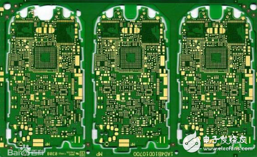
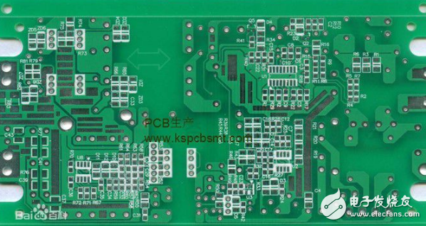
PCB, short for Printed Circuit Board, is an essential electronic component used as a base for mounting and connecting various electronic parts. It serves as the foundation that supports and electrically connects different components. The term "printed" comes from the process of printing the circuit patterns onto the board, hence the name "printed circuit board."
The PCB Manufacturing Process:
1. Contacting the Manufacturer
The first step is to reach out to a PCB manufacturer. You’ll typically need to register as a customer, receive a quote, place an order, and then track the production timeline accordingly.
2. Material CuttingPurpose: Based on the engineering data (MI), large sheets are cut into smaller pieces that meet the customer’s specifications. This ensures that each piece is ready for further processing. Process: Large sheet material → cutting according to MI requirements → sawing → beveling or edging → final inspection and exiting the board.
3. DrillingPurpose: Holes are drilled at specific locations based on the engineering data to allow for component placement and electrical connections. Process: Stack pin → loading the board → drilling → unloading → inspection and repair if needed.
4. Copper Deposition (Through-Hole Plating)Objective: A thin layer of copper is chemically deposited on the walls of the holes to ensure conductivity. Process: Surface roughening → hanging the board → automatic copper plating → unloading → dilute sulfuric acid dip → thick copper plating.
5. Image TransferPurpose: This step transfers the circuit pattern from the film to the board. Process (Blue Oil Method): Board grinding → printing on one side → drying → printing on the other side → drying → exposure → shadowing → inspection. (Dry Film Method): Board preparation → lamination → standing → exposure → development → shadowing → checking).
6. Graphic PlatingPurpose: Electroplating is applied to the exposed copper areas or hole walls to build up a desired thickness of copper, gold, or tin. Process: Loading the board → degreasing → washing → micro-etching → washing → pickling → copper plating → washing → pickling → tin plating → washing → unloading.
7. Desmear / Resist RemovalObjective: Removes the protective coating using a sodium hydroxide solution to expose the non-copper areas. Process (Water Film): Inserting the board → alkali soaking → washing → scrubbing → passing through the machine. (Dry Film): Place the board → pass through the machine.
8. EtchingPurpose: Chemical etching removes unwanted copper from the board, leaving only the desired circuit pattern. Process: After the image transfer, the board is immersed in an etching solution to dissolve the excess copper.
Purpose: The solder mask protects the copper traces and prevents solder from flowing onto unintended areas during assembly. Process: Board grinding → printing photosensitive solder mask → laminating → exposure → shadowing. For double-sided boards, the process is repeated on both sides after baking.
10. Character PrintingPurpose: Adds markings such as part numbers, logos, or identifiers for easy identification. Process: After the green oil is applied, the board is cooled, the network is adjusted, characters are printed, and the board is finalized.
This detailed manufacturing process ensures that the PCB meets the required specifications and performs reliably in electronic devices. Whether it's a rigid PCB or a flexible one, the core steps remain similar, though some variations may occur depending on the design and materials used.computer keyboard accessories,mechanical keyboard accessories,gaming keyboard parts,custom keyboard parts
Dongguan Yingxin Technology Co., Ltd. , https://www.dgyingxintech.com