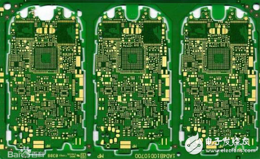
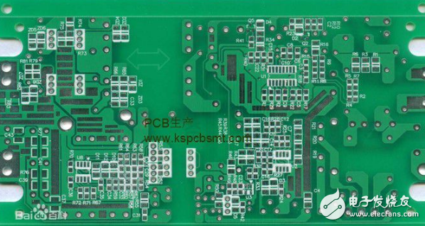
**First, Printed Circuit Board (PCB)**
A PCB, or Printed Circuit Board, is a fundamental electronic component used to support and connect various electronic parts. It serves as the base for mounting and linking components through conductive pathways. The term "printed" comes from the process of printing these circuits onto the board using specialized techniques.
**PCB Manufacturing Process:**
**1. Contact the Manufacturer**
The first step in the PCB manufacturing process is to reach out to a reliable manufacturer. Once you’ve registered your account, a representative will provide a quote, and you can proceed with placing an order. After that, you’ll be kept updated on the production timeline.
**2. Material Cutting**
Purpose: Based on the engineering data (MI), large sheets are cut into smaller pieces that meet the customer’s specifications.
Process: Large sheet material → cutting according to MI → sawing → rounding edges → final inspection and exiting the board.
**3. Drilling**
Purpose: Holes are drilled at specific positions on the board according to the design requirements.
Process: Aligning pins → loading the board → drilling → unloading → inspecting and repairing any issues.
**4. Copper Deposition (Sinking Copper)**
Objective: A thin layer of copper is chemically deposited on the walls of the holes to ensure proper conductivity.
Process: Surface roughening → hanging the board → copper plating → rinsing → dilute sulfuric acid treatment → thick copper plating.
**5. Image Transfer**
Purpose: This step involves transferring the circuit pattern from the film to the board.
Process: For the blue ink method: board cleaning → printing one side → drying → printing the other side → exposure → development → inspection. For the dry film method: board preparation → lamination → exposure → developing → inspection.
**6. Graphic Plating**
Purpose: Copper, gold, or tin is electroplated onto the exposed areas of the board to achieve the desired thickness.
Process: Loading the board → degreasing → washing → micro-etching → washing → pickling → copper plating → washing → pickling → tin plating → washing → unloading.
**7. Stripping**
Objective: Remove the anti-plating coating using a sodium hydroxide solution to expose the copper areas.
Process: Water film: inserting → alkali soaking → washing → scrubbing → passing through the machine; Dry film: placing the board → passing through the machine.
**8. Etching**
Purpose: Chemical etching is used to remove unwanted copper from non-circuit areas.
**9. Solder Mask (Green Oil)**
Purpose: The solder mask is applied to protect the copper traces and prevent solder from flowing onto them during assembly.
Process: Board cleaning → applying photosensitive green oil → laminating → exposure → development; or printing on both sides and baking.
**10. Marking (Characters)**
Purpose: Adding characters or logos helps identify the board easily.
Process: After the green oil is applied → cooling → network adjustment → printing characters → final inspection.
This detailed process ensures that each PCB is manufactured precisely, meeting the required specifications for performance and reliability. Whether it's a simple single-layer board or a complex multi-layer PCB, understanding the steps involved helps in making informed decisions when choosing a manufacturer or designing a circuit.
upper case aluminum,keyboard frame,keyboard case hot swappable,customizable keyboard case
Dongguan Yingxin Technology Co., Ltd. , https://www.dgyingxintech.com