1 Introduction
As we all know, Class AB audio amplifiers have higher efficiency than Class A (generally around 50%), and lower crossover distortion than Class B [1]. They are widely used in various mobile phones and MP3 portable devices The main force in the audio amplifier market 
The output op amp is the core part of the audio power amplifier chip, accounting for most of its layout area. Its performance and integration directly affect the performance parameters and the size of the entire audio power amplifier chip.
In recent years, with the widespread application and continuous development of portable devices such as mobile phones, PDA, MP3, MP4, etc., the requirements for audio power amplifier chips have also become higher and higher High performance, low power consumption and high integration are its development direction And this is also a requirement for the output operational amplifier module
Based on the N-well CM () S process, this paper uses the 0.6 μm DP-DM process to design a small static power consumption, small input offset voltage, high gain, high common mode rejection ratio and power supply rejection ratio. Large output swing, high bandwidth, and very low THD output power operational amplifier, suitable for most class AB audio power amplifier chips
2 Circuit design
The whole circuit is divided into two stages, the first stage is a differential input circuit, and the latter stage is a power tube push-pull output
2.1 The choice of op amp structure
For the output power operational amplifier, the design focus is on the differential input circuit of the previous stage, hoping to have the highest possible open-loop gain and unity gain frequency, while also considering speed, common mode rejection ratio, power supply rejection ratio, power consumption, etc Restrictions on performance
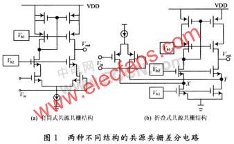
The differential circuit with cascode structure has a very high voltage gain, which is equivalent to the two-stage op amp with simple structure, and has better frequency characteristics. In the literature [2] compared three different structures of differential circuits Now there are two common cascode structures, sleeve type and folding type, as shown in Figure 1 Figure 1 (a) is a sleeve type cascode differential op amp. Its advantages are good frequency characteristics and low power consumption [2] The disadvantage is that there are too many "stacked" tubes on the branch, resulting in a small input common-mode level range and output swing, which is not suitable for working at low voltage. Figure 1 (b) is a folded cascode differential op amp, whose frequency characteristics are equivalent to the sleeve type [2] Compared with the sleeve type, the main advantage is that it has a larger input common mode level range, because it does not "stack" a common source cascode tube at the upper end of the input tube, and a larger output swing The disadvantage is that the input to the tube requires an external bias current, which consumes more power
From an application point of view, in the above two op amp structures with comparable voltage gain and frequency characteristics, the sleeve structure requires a higher power supply voltage and the limitations in the input common mode level range, making it unsuitable for application in power amplifiers Input stage circuit Although the folded cascode structure has greater power consumption, it is more suitable for the design requirements here And the minimum power supply voltage he requested is also within the acceptable range
 |
2.2 Bias circuit
The low-voltage cascode current mirror structure used in the bias circuit not only has the advantage of accurately replicating the current by the common cascode current mirror, but also can work at a lower power supply voltage than the common cascode current mirror [3] as shown in picture 2
 |
The minimum voltage margin consumed by the cascode current mirrors M3 to M4 of this structure is the sum of their overdrive voltages, and it can accurately mirror the Iref The input range of the bias voltage Vb is: ![]()
2. 3 overall circuit
In the overall circuit of the op amp of FIG. 3, FIG. 3 (a) is the main body of the op amp, including a differential input circuit and a power tube Mp, Mn push-pull output stage, Figure 3 (b) is his bias Circuit, providing bias voltage of Vb1 ~ Vb8
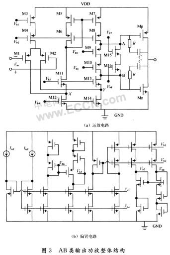 |
The differential input circuit has a folded cascode structure. In the figure, M1 and M2 are input pair tubes, respectively "+" and "+" input terminals, and M3 and M4 are the mirror parts of the low-voltage cascode current mirror. Provide tail current source Compared with Figure 1 (b), the only difference is that four tubes M9, M10, M15, and M16 are inserted between the output terminals of the differential circuit, that is, M8 and M13. The gate voltages of the power transistors Mp and Mn make Vgsp slightly less than Vthp and Vgsn slightly less than Vthn at zero differential input. Mp and Mn all work in the sub-threshold region and a certain current flows This is the basic feature of class AB amplifiers, as far as possible to eliminate crossover distortion In order to provide a large output current, their width-to-length ratio is large (a lot of the same tubes are connected in parallel on the layout, and the number of P tubes in parallel is about 3 times that of N tubes, so that the current flowing through the load in a cycle is equal )
In differential input, when the "+" terminal inputs a higher level, the current of the M2 branch decreases rapidly, and the current flowing through the M5 and M7 branches remains equal, so the current flowing through M14 is less than the current flowing through M12, Force M14 to work in the linear region, the voltage at point Y is very low, in order to keep the branch current unchanged, M13 enters the deep linear region, VB drops sharply At the same time, the M16 and M15 branch currents increase, and the M10 and M9 branch currents decrease, resulting in a decrease in VA Eventually, VB drops to a very low level, VA follows VB, M10, M9 cut off, M16, M15 enter the linear zone At this time, Mn is off and Mp is on Similarly, when the "-" end loses to a higher level, Mn is turned on and Mp is turned off The output voltage swing is:
![]()
The low-frequency voltage gain of the op amp can be roughly calculated as follows: ![]()
AV1 is the gain of the first differential circuit M9, M10, M15, M16 have little effect on the gain, and its effect can be ignored, so: ![]()
AV2 is the gain of the second push-pull output stage: ![]()
Among them, the width-length ratio of the output power tube is adjusted so that Mp is about 3 times of Mn, so that the above formula is established
For such a multi-pole two-stage op amp, Miller compensation is performed in series with the output resistance and capacitor to increase the phase margin and improve stability Through frequency compensation, the two main poles are [1]:
Where RA is the total impedance from point A (or B) to ground, CA is the total parasitic capacitance from point A (or B) to ground, and Cι is the total capacitance at the output
p1 is the closest to the origin and is the pole generated by point A; p2 is the pole at the output and is far from the origin At the same time, due to the resistance and capacitance forming a path, a zero point is generated [1]:
![]()
Adjust R appropriately so that Z = p2, which cancels with the second main pole, increasing the bandwidth
2.4 Working environment
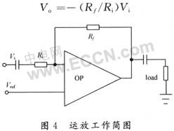
Use single power supply, work in closed loop state The reference voltage is VDD / 2 As shown in Figure 4 The closed-loop transfer function is:
 |
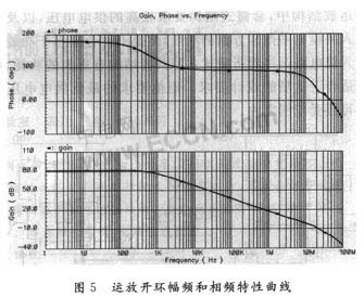
3 Simulation results
The simulation performance parameters are shown in Table 1.
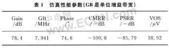 |
Figure 5 and Table 1 are the simulation results, which are measured under open-loop and no-load conditions The simulation tool is Cadence Spectre, using a 0.6 μm N-well CMOS process model, the simulation environment is VDD = 5 V, T = 27 ℃, typical conditions The above results show that the unity gain bandwidth GB is 7.941 MHz, the phase margin is 74.60, and the frequency characteristics are good; the offset voltage is very small, 38.92 μV; there is a higher voltage gain, common mode rejection ratio, and power supply Rejection ratio; in addition, when the input amplitude is 1 V and the frequency is 1 kHz sine wave, the output THD is very small, 0.004%
 |
4 Conclusion
The class AB output power amplifier circuit designed in this paper uses a folding cascode structure, a power tube push-pull output, and uses an external current source for power supply, and a low voltage cascode current mirror structure bias circuit The simulation structure shows that the operational amplifier has the characteristics of high gain, low input offset voltage, low THD, etc. At the same time, it has good frequency characteristics and low static power consumption, which meets the requirements of a high-performance class AB audio power amplifier chip It can be seen that the design is almost satisfactory, and small adjustments can also make each tube work in the most stable working area by changing the W / L ratio
Our UL Certified Switches are mainly 3 Position Key Switch with 19mm Installation size. This series is a representative , competitive and hot product in our products catalog.
UL Certified Electric Key Switch, which indicates the Key Switches that have UL certification. The UL Safety Laboratory is the most authoritative in the United States and the largest private institution in the world for safety testing and identification.

Our company has UL certification testing equipment, so that UL certification series Key Lock Electrical Switches products meet international standard so could meet our customer`s needs. We are devote to supplying high-quality and excellent products to our customers with the Quality management testing, supplier management, feed inspection, in-process inspection, finished product inspection, measurement ,instrument management, final personnel training , high-class quality concepts.
We are always insisted on the quality of the Key Lock Switch, so our key switches with supreme quality could be investigated. If the client receive abnormal quality, the quality team meeting will be held actively to rigorously analyze the cause of the Abnormal product and make the correct solution. The same batch of materials should be separated in time to ensure that similar quality anomalies wont happen again, so we could achieve the goal that corrective and preventive measures are taken to make efficient solutions for the UL series of Key Switches used by customers.

UL Certified Switches
Ul Certified Switches,Ul Certified 16Mm Switch ,Ul Certified Waterproof Switch,Ul Certified Electric Power Switch
YESWITCH ELECTRONICS CO., LTD. , https://www.yeswitches.com