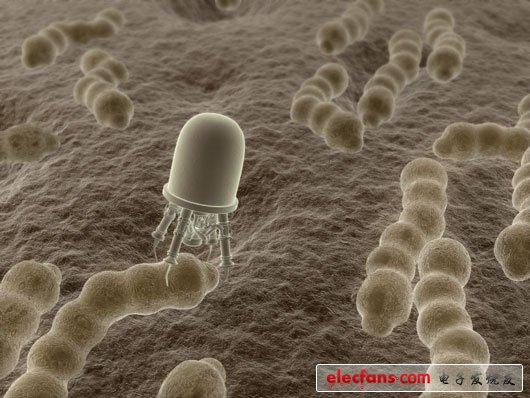
Panasonic and the Belgian Microelectronics Research Center (IMEC) have jointly developed a fully automatic small gene detection chip that can complete the test in 1 hour. The chip can use several μL of blood to detect genetic information such as SNP (Single NucleoTIde Polymorphism). SNP refers to the existence of different types of bases in the genomes of different individuals. By detecting SNP, you can diagnose the presence or absence of genetic diseases and the future risk of genetic diseases, and you can determine the genes related to the disease.
Most of the previous automatic gene detection devices are large-scale devices, and most of them adopt the method of sending the specimen to a special testing institution for analysis. Therefore, the test results have to wait a few days to a week or so to be known. The chip developed this time is different. It only takes 1 hour to complete the test including the pre-treatment process. Therefore, at the clinical site, doctors can make judgments on the patients' medication and risk of disease on the spot.
The chip developed this time integrates the function of extracting and amplifying DNA from a small amount of blood for SNP judgment. Specifically, an ultra-small pump that transports blood and medical fluid, a DNA extraction and amplification section, a high-precision filter, and a high-sensitivity sensor are integrated on a chip of about 9 cm2.
The necessary technologies newly developed to realize the chip are roughly the following three items.
(1) Ultra-small high-pressure pump using conductive polymer actuators
By laminating a polymer film on a silicon substrate, a polymer actuator that can greatly expand and contract in the lamination direction was developed, and a diaphragm pump that transported liquid by moving the diaphragm was realized. The polymer actuator can generate a pressure of more than 300 atmospheres, and can easily move the solution including the injection of liquid into the high-precision filter membrane for DNA screening in the micro-channel. In addition, low-voltage (1.5V) operation that can be driven by a battery is realized.
(2) High-speed PCR technology
When performing genetic diagnosis, it is necessary to remove the region containing SNP from the DNA and increase it to a certain amount. Generally, a method called PCR (Polymerase Chain ReacTIon, polymerase chain reaction) is used to amplify the DNA, but the original PCR It takes 2 hours to amplify DNA. Therefore, the researchers used a silicon substrate with good thermal conductivity to optimize the means of isolating the surrounding heat, improve the temperature follow-up of the temperature rise and fall, and also realize the structure of causing the PCR reaction with a small amount of liquid. These measures reduce the time required to amplify DNA to less than 15 minutes.
(3) High-precision, high-sensitivity electrochemical sensor
When identifying SNPs electrically, it is necessary to use expensive special electrodes in which artificial DNA for identification is fixed to the electrodes. With the newly developed sensor this time, it is possible to electrically recognize SNPs in a state of being dissolved in a small amount (about 0.5 μL) of chemical liquid without fixing identification artificial DNA on electrodes.
HDI is the English abbreviation for High Density Interconnector. High-density interconnect (HDI) manufacturing is one of the fastest growing areas in the printed circuit board industry. From the first 32-bit computer from HP in 1985 to the large client server with 36 sequential multi-layer printed boards and stacked micro-vias, HDI/mini via technology is undoubtedly the future PCB architecture. Smaller ASICs and FPGAs with smaller device spacing, I/O pins, and embedded passives have shorter rise times and higher frequencies, all of which require smaller PCB feature sizes, which drives Strong demand for HDI/mini vias.
HDI process
First-order process: 1+N+1
Second-order process: 2+N+2
Third-order process: 3+N+3
Fourth-order process: 4+N+4
Buried Hole Pcb,Blind Hole Pcb,Buried Blind Hole Pcb,Multilayer Blind Buried Hole Pcb
Chuangying Electronics Co.,Ltd , https://www.cwpcb.com