Silicon is the most commonly used material in the microelectronics industry, but because it has an indirect bandgap, the luminous efficiency is very low. Recently, a research team led by Prof. Chen Minjun and Professor Yang Zheren from the Department of Materials Science and Engineering, National Taiwan University, used n-type zinc oxide/silica-silicon nanocrystal-silica/p-type silicon substrate (n- The heterostructure of ZnO/SiO2-Si nanocrystal-SiO2/p-Si) has successfully produced high-efficiency silicon light-emitting diodes, opening a new opportunity for the application of non-direct-band semiconductors in optoelectronics.
The Taiwan University team first used silicon low-temperature chemical vapor deposition (LPCVD) to grow silicon nanocrystals on a p-type silicon substrate, and then embedded the crystallites in the silicon dioxide layer by thermal oxidation. Then, a high-quality n-type ZnO thin film was formed by Atomic Layer Deposition (ALD), which was used as a transparent conductive layer, an electron injecting layer, and an antireflection layer capable of improving light extraction rate. ALD is an advanced nano-film deposition technology that can control the thickness and composition of thin films with atomic precision. It also has high uniformity, low defect density, large-area batch production, and low deposition temperature. .

Electron micrographs clearly show that silicon nanocrystals with a diameter of about 24 nm are embedded in a silicon dioxide layer with a thickness of about 9.2 nm. The electron and the hole are respectively formed by an n-type ZnO thin film and a p-type silicon substrate, tunneling through the silicon dioxide layer into the silicon nanocrystallite. Since the electron hole pair is confined in the narrow crystallites, and the silicon dioxide has a repairing effect on the surface defects of the crystallites, the electron hole has a large probability of generating a re-radiation, and a transparent ZnO film is added. The anti-reflection effect greatly increases the luminous efficiency of the silicon light-emitting diode.
The peak temperature of the room temperature luminescence spectrum of the above components is at a wavelength of 1140 nm, and the energy is very close to the energy gap of silicon, corresponding to the physical mechanism of phonon-assisted indirect carrier recombination. The researchers also measured the luminescence power when different DC currents were injected. The external quantum efficiency of this module is as high as 4.3×10⁻⁴ at room temperature, 100 times that of bulk silicon as the substrate, and the internal quantum efficiency is estimated to be about 10-3, breaking the limit of indirect band semiconductors.
It is worth mentioning that the process and structure of this component are fully compatible with the current VLSI technology and can be directly integrated into current integrated circuits. The results of this research are expected to be applied to optical interconnections in integrated circuits and high-performance silicon light-emitting diodes required for photonic integrated circuits.
The Taiwan University team first used silicon low-temperature chemical vapor deposition (LPCVD) to grow silicon nanocrystals on a p-type silicon substrate, and then embedded the crystallites in the silicon dioxide layer by thermal oxidation. Then, a high-quality n-type ZnO thin film was formed by Atomic Layer Deposition (ALD), which was used as a transparent conductive layer, an electron injecting layer, and an antireflection layer capable of improving light extraction rate. ALD is an advanced nano-film deposition technology that can control the thickness and composition of thin films with atomic precision. It also has high uniformity, low defect density, large-area batch production, and low deposition temperature. .

Electron micrographs clearly show that silicon nanocrystals with a diameter of about 24 nm are embedded in a silicon dioxide layer with a thickness of about 9.2 nm. The electron and the hole are respectively formed by an n-type ZnO thin film and a p-type silicon substrate, tunneling through the silicon dioxide layer into the silicon nanocrystallite. Since the electron hole pair is confined in the narrow crystallites, and the silicon dioxide has a repairing effect on the surface defects of the crystallites, the electron hole has a large probability of generating a re-radiation, and a transparent ZnO film is added. The anti-reflection effect greatly increases the luminous efficiency of the silicon light-emitting diode.
The peak temperature of the room temperature luminescence spectrum of the above components is at a wavelength of 1140 nm, and the energy is very close to the energy gap of silicon, corresponding to the physical mechanism of phonon-assisted indirect carrier recombination. The researchers also measured the luminescence power when different DC currents were injected. The external quantum efficiency of this module is as high as 4.3×10⁻⁴ at room temperature, 100 times that of bulk silicon as the substrate, and the internal quantum efficiency is estimated to be about 10-3, breaking the limit of indirect band semiconductors.
It is worth mentioning that the process and structure of this component are fully compatible with the current VLSI technology and can be directly integrated into current integrated circuits. The results of this research are expected to be applied to optical interconnections in integrated circuits and high-performance silicon light-emitting diodes required for photonic integrated circuits.
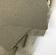
EMI shielding Z conductive foamUsing vacuum coating and composite
plating method,coating copper and nickle on open cell pu foam and combine with
two layer of mesh material. X-Y-Z all sides conductive , very good for customer
need z conductive.
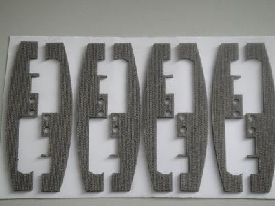
For die cutting,making I/O or D-Sub gasket,and
other EMI-RFI shielding gaskets or
contacts. It is an economic solution for EMI shielding problems .
We could backing adhesive or die cut for the customers, any other questions,please contact with us.


Conductive Foam
Conductive Foam,Emi Shielding Foam,Rfid Conductive Foam,Emi Shielding Conductive Foam
JINAN EMI SHIELDING TECHNOLOGY CO., LTD. , http://www.emirfi.com