Summary:
The focus is on the testing and implementation of flying needle online testing technology in electronic module testing. This paper introduces the flying needle test principle, expounds the flow of the electronic module flying probe test and the electronic module in the test, proposes the solution to the problem in the short circuit test, and the quick modification technique of the NOD file, and details the flying needle and the needle. The complementary relationship of the beds. The use of flying probe testing technology can accurately locate the fault point and shorten the debugging cycle, which plays an important role in the debugging of mass production electronic modules.
With the continuous enhancement of the functions of electronic modules, the integration is getting higher and higher, the device is small in size and high in density, which increases the difficulty of manual inspection and the difficulty of debugging, especially for multi-variety, mass production, because there is no high-integration electronics. The module's testing technology and manual manual detection methods have severely restricted the rapid development and production of electronic modules. Therefore, the automation and mechanization of electronic modules after welding are replaced by manual testing. Flying needle detection is a flying needle detection system that uses a stepping motor to control the flying needle to realize the flying needle motion measuring board. It is the latest solution to some major problems of the current electronic module. This article will introduce the detection principle of the flying probe test and how to use the flying probe tester to test the electronic module.
1 Structure and principle of the flying probe test system
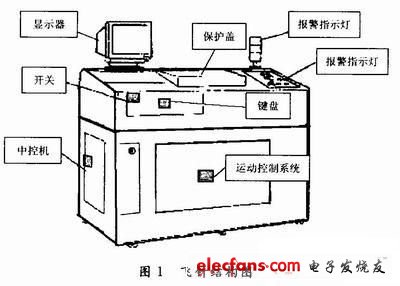
The flying probe test is one of the methods for checking the quality of electronic module soldering on-line. It is a system for testing the solder joints of electronic modules in the manufacturing environment. It replaces the traditional needle bed with a probe and is equipped with high-speed movable on the XY mechanism. 4 probes, when working, manually put the measuring unit into the testing machine, and touch the test pad and the via hole through the probe of the flying probe tester to test the welding effect of the components in the measuring unit. The test probe is connected to the driver (signal generator, power supply, etc.) and the sensor (digital multimeter, frequency counter, etc.) through a multiplex system to test the components on the unit under test. When a component is being tested, it is under test. The other components on the unit are electrically shielded by the probe to prevent reading interference. The structure of the flying probe is shown in Figure 1.
The flying probe tester can test the resistance, capacitance value, inductance value of the electronic module, common devices such as diodes, transistors, and three-terminal regulators. It can also test integrated circuits, short circuits and open circuit tests.
2 implementation of flying probe tester
In order to realize the real-time monitoring of the welding quality of the electronic module after welding, to master the welding quality of each electronic module, the flying needle tester is required to test the electronic module, and the short circuit, open circuit phenomenon and damage of the tested component are detected by flying probe test. The device is eliminated, and the test and debugging process is usually as shown in Figure 2.
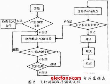
In the process of achieving the target, the EDA design process file will generate a netlist file in ASCII format, which will be converted into the NOD file of the electronic module under test. The NOD file will be sorted and modified to produce the source file. The source file is modified according to the parameter requirements of the electronic module, and then the software that is expected to be compiled is processed. Use the camera to make coordinate transformation points, generate MRK and MZF files, and set the coordinate conversion points to check whether the test point settings are appropriate. The choice of test points is combined with the change of the NOD file. The process of checking the test points is also a process of modifying and correcting the test points. Finally, select the statement that needs to be debugged. Each type of component corresponds to its own debugging statement, and the debugged statement is modified, that is, the parameters such as the isolation point and voltage of the device under test are set, and the modified operation is performed until the test requirements are met. The processing of the NOD file is the most cumbersome. The following describes how to quickly modify the NOD file. The file format is as follows:
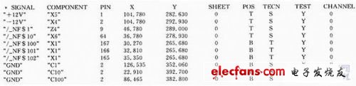
The last column is the channel number of the solder joint of the tested part, which needs to be modified manually. The modification method is:
(1) Modify CHANNEL, from top to bottom, according to the name of SIGNAL, the name is the same as CHANNEL changed to natural number 1, when the name of SIGNAL is changed, then CHANNEL is changed to natural number 2, and then look down until there is Other differences, continue to accumulate.
(2) For parts that are not tested or affect the operation of the probe, the “TEST†attribute should be changed from “F†to “N†(not tested) in the *.NOD file. Such as the vias that are not filled with tin after the electrical installation, around the programming pins, around the higher components, and chips with socket conversion soldering.
The common processing method is to manually modify one by one. After the modification is completed, the proofreading is one by one. The disadvantage is that the efficiency is low and error-prone. In order to change this situation, it is necessary to find a way to improve efficiency. Adjust the modification method:
(1) Open the *.NOD file with Notepad and copy all the contents into the WORD document;
(2) Delete the first line ("* SIGNAL COMPONENTPIN XY SHEET POS TECN TEST CHANNEL");
(3) Select all (Ctrl+A) data;
(4) Click on the form\Insert form (put the data in the form);
(5) All the forms are selected and copied to the Excel form;
(6) Use the convenient operation of the Excel table to number the tenth column. The method is: starting from 1, the different signal names (refer to the first column) are incremented by 1 and saved after completion;
(7) Then modify the penultimate column by: all filling with "Y" first, according to the selection rules and error conditions, changed to "F" (mandatory) or "N" (not tested), and saved after completion;
(8) Select all (Ctrl+A), copy (Ctrl+C);
(9) Open the *.NOD file with Notepad, only keep the first line and delete it. Paste (Ctrl+V) the contents of the clipboard from the second line, save, and the change is completed.
The modified processing method utilizes the convenience of the processing of the Office software, and effectively improves the processing efficiency of the NOD file.
Custom PCB Assembly = Custom Printed Circuit Board Assembly, which means the PCB Board is customized as the customer required and designed. Zhongfeng would manufacture the PCB boards follow the design file, source the components follow the BOM file and do the PCB Assembly job follow the assembly drawing and the pick&place file. After PCB assembly done, the components would be mounted on the PCB boards tightly and connected each other through the copper circuits. We call such board as PCBA board or custom PCBA board.
Depends on the components assembly types, it have THT PCB assembly, SMT PCB Assembly , one sided SMT and THT PCB assembly, two sided SMT and THT PCB assembly.
Depends on the PCB type, it have Rigid PCB Assembly , Flex PCB Assembly and Flex-Rigid PCB Assembly.
Also we would call some PCB assembly types as Prototype PCB Assembly, Mass PCB Assembly , Turnkey PCB Assembly, LED PCB Assembly and BGA PCB Assembly , etc.
With our 15years professional experience, we are available for all types of PCB assembly service from prototype to mass production, available for 01005, 0201, 0.3mm BGA, 0.3mm QFP.
PCB Assembly Capabilities
|
Quantity |
1 pcs - 1,000,000 pcs |
|
Assembly type |
SMT, THT or Hybrid |
|
Parts procurement |
Full turnkey (ZhongFeng provide all components) |
|
Partial turnkey ( Customer provide the main components and ZhongFeng provide the rest) |
|
|
Kitted (Customer provide all components) |
|
|
Component types |
SMT 01005, 0201, BGA 0.3mm pitch, QFP 0.3mm pitch, etc. |
|
Test |
Visual Inspection, AOI, Custom testing, ICT, FCT, Test jig |
PCB Assembly Products Show

PCB SMT Assembly Factory Show


Custom PCB Assembly
Custom PCB Assembly,Circuit Board PCB Assembly,Surface Mount PCB Assembly,Quick PCB Assembly
ZhongFeng Electronic Technology Co., Limited , https://www.dopcba.com