IntroductionThe DS1856 uses internal calibration and right shifting (Scalable Dynamic Ranging) to enhance the built-in 12-bit ADC. This gives the DS1856 the precision and accuracy of a 16-bit ADC without added size and cost. Plus, the device's programmable gain and offset functions can reduce, or even eliminate the need for external signal-conditioning circuitry. Once calibrated, these functions convert the analog input signal to a digital value without requiring any action from the user.
The DS1856 functions similar to the DS1859, but has a memory map compatible with the DS1852 memory structure. The DS1856's internal calibration procedure is also quite similar to that for the DS1859. (For examples of the DS1859 internal calibration, refer to Application Note 2858. ) However, the DS1856 has different Table assignments, as well as a slightly different equation for calculating the offset register values.
This application note explains the internal calibration procedure for the DS1856, and how using this function can benefit the application. This note also provides procedures for determining and implementing the internal calibration and right-shifting features of the DS1856. A Note about Password AccessThe settings for the Scale and Offset values ​​for the three MON inputs are located in Table 03 of the DS1856. To read or write to these values, level-2 password access (PW2) is required. This access is granted if the password for PW2 level entry is entered into the password entry bytes (PWE located in addresses 7Bh-7Eh) using one, 4-byte WRITE command. DS1856 Analog Monitor InputsLike the DS1859, the DS1856 has three analog inputs. These inputs, MON1, MON2, and MON3, can be used to monitor such signals as Tx Power, Rx Power, and Tx Bias. The block diagram in Figure 1 shows the structure of the MON inputs.
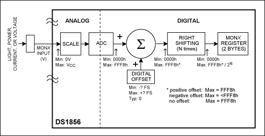
Figure 1. DS1856 MON input block diagram.
The input block of the MON pin is composed of an analog and digital portion. In the analog portion, a single-ended voltage is connected to the MON pin. This voltage is then sent to the Scale block, which is capable of attenuating or applying a gain to the input voltage. Setting the Scale value allows a desired LSB, or full-scale voltage, to be set. The full-scale voltage is the voltage that produces a value of FFF8h in the corresponding MON register. By setting the Scale's value for each MON input's Scale value, the gain of those signals can be controlled to make the best use of the ADC.
The 12-bit ADC follows the Scale block. The conversions from the ADC are digital outputs that are left justified. Each output is a 16-bit value with the three LSBs internally masked to 0. This allows the ADC to output values ​​from 0000h to FFF8h.
The ADC's digital output is then further adjusted by the programmable Offset value. Positive or negative offsets can be applied to the ADC output by digital addition or subtraction. These adjustments are still clamped at values ​​of 0000h and FFF8h.
The last adjustment to this signal is made by using right shifting. The Right-Shifting register stores a 3-bit value used to shift each MON value from 0 to 7 spaces to the right. This makes better use of the ADC range and increases the accuracy of the readings. Right shifting is the last function performed on the MON signal before the digital value is sent to the MON register.
Once the digital value of the MON signal is determined, internal warning and alarm limits compare their values ​​to the digital MON value. Warning and alarm flags are set / reset accordingly. Factory Calibrated DS1856Each DS1856 is calibrated at the factory to produce FFF8h in the MON registers when 2.5V is applied to the corresponding MON input pin. The Offset registers for each MON input are set to zero so that when 0V is applied to a MON pin, the digital output 0000h will be read for that MON input. The default value of the Right-Shifting register is 0, thus no right shifting will occur.
Given this factory trim, the DS1856 will produce one of 4096 digital values ​​for MON input voltages in the range of 0 to 2.5V. This is a resolution of 610µV (2.5V / 4096) for the 12-bit conversion. However, not all applications will use this range and may only apply a maximum voltage of 0.5V. In those instances, only 820 possible digital values ​​will be produced, leaving 3276 values ​​that will never be used. While the resolution is still 610µV, the 12-bit converter is not used efficiently.
To make better use of the 12-bit converter, the DS1856 MON value must be recalibrated to a full-scale voltage of 0.5V. To do this, right shifting must be used in addition to adjusting the scale and offset values ​​as described in the The following section. How to Use the DS1856 Internal Calibration and Right ShiftingThe best use of internal calibration and right shifting is when the MON input signal is small (smaller than 2.5V) and not using much of the default ADC range. By adding a gain to the analog signal and then dividing that signal down in the digital domain, the desired LSB is maintained and more of the ADC range is used. With this method, both precision and accuracy are improved by a factor of two for every right shift (up to a maximum of 4 shifts). After four right shifts, the digital output begins to lose precision, but the accuracy continues to improve.
Figure 2 is an excellent example of how to make good use of internal calibration and right shifting. The first plot, A, shows the example signal to be monitored. The maximum voltage applied to the MON input is 0.5V. Plot B shows the factory -calibrated transfer function, and plot C shows the transfer function using two right shifts and a full-scale voltage set to 0.625V (2.5V / 4). With a full-scale voltage of 0.625V, more of the digital codes will be used compared to using a full-scale voltage of 2.5V. The resulting conversions will be four times larger than the 2.5V full-scale voltage. However, by using the right shifting function, those conversions are divided back down by a factor of four (two right shifts).
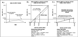
Figure 2. Right-shifting comparison. (Click for larger image)
As all three plots in Figure 2 show, the same y-axis can be used as a point of comparison. The horizontal line drawn through all three plots represents the maximum-input voltage level to be applied to this pin. By comparing plots B and C, the benefit of right shifting can be seen. Plot B shows how much of the digital output range is wasted by not using internal calibration and right shifting. Plot C shows how internal calibration and right shifting can be used to regain that lost range and Increase signal accuracy. Determining the Number of Possible Right ShiftsTwo factors determine the number of right shifts that can be used. One factor is a function of the full-scale voltage. The other factor is the percentage of digital codes used. If the maximum voltage and full-scale voltage of the MON signal are known, then the digital output values ​​can be calculated. Otherwise, a trial-and-error method will be necessary to determine the ideal number of right shifts. The following steps detail th e trial-and-error method. Set the right shift bits to 0. Internally calibrate the part to yield the desired LSB, which will determine the initial full-scale voltage. Apply the minimum and maximum input signal, then read the corresponding digital outputs to determine the digital code range used. Determine what percentage of the ADC range is used. If the digital readings are between FFF8h and 7FF8h, then right shifting should not be used, and the number of right shifts should be set to 0. If the digital readings are between 7FF8h and 3FF8h, then one right shift can be used. If the digital readings are between 3FF8h and 1FF8h, then two right shifts can be used, etc. Refer to Table 9 in the DS1856 data sheet for the remaining ranges. If right shifting is used to make more efficient use of the ADC range, then the gain must be calibrated so that the desired LSB (full-scale voltage) is maintained. The adjusted gain (scale value) is calculated by using the formula: new full-scale voltage = ini tial full-scale voltage / 2 # of right shifts. If, for example, the internal calibration from step 2 above resulted in a full-scale voltage of 2.0V (to obtain the desired LSB), and digital readings were greater than 1FF8h but never exceeded 3FF8h, two right shifts would be used. The new full-scale voltage for this example is 2.0V / 22 = 0.5V. With the right shift value set to 0, calibrate the MON channel to the new full-scale voltage. Set the right shift bits to their new value. Once the evaluation determines the ideal number of right shifts and the full-scale voltage for a particular application, only steps 1, 6, and 7 are needed for production calibration. DS1856 Internal Calibration and Right -Shifting RegistersThe DS1856 registers that hold the calibration settings (Scale, Offset, and Right Shifting) as well as the digital readings for each of the analog inputs are summarized in Table 1. Addresses are shown for each of the MON channels as well as VCC . (VCC is included in the table for co mpleteness, although it will not be discussed in this application note.) The locations of the digital conversions are included to show their relative placement. Notice that the Scale, Offset, and Right-Shifting registers are located in memory Table 03h in the DS1856. Table 03h is selected by writing 03h into the Table Select byte, 7Fh. As the digital conversions are in the lower bank of memory (0 to7Fh), they are independent of the Table Select byte value.
Table 1. DS1856 Internal Calibration and Right-Shifting Registers
| VCC | MON1 | MON2 | MON3 | |
| Scale Cal | 92h to 93h | 94h to 95h | 96h to 97h | 98h to 99h |
| Offset Cal | A2h to A3h | A4h to A5h | A6h to A7h | A8h to A9h |
| Right Shifts | N / A | 8Eh (b6-b4) | 8Eh (b2-b0) | 8Fh (b6-b4) |
| Readings | 62h to 63h | 64h to 65h | 66h to 67h | 68h to 69h |
| Table 03h | ||||
It is important to note when calibrating the DS1856 that the values ​​of both the Offset and the Right-Shifting registers must be known. Otherwise, if those values ​​are some non-zero value and the value stored in the Scale Cal register does not consider those Offset and Right Shifting values, the device will not be properly calibrated.
Offset Cal RegisterThe DS1856's offset is a digital addition to, or subtraction from the converted values ​​generated by the ADC. The two-byte Offset Cal value is programmed after the scale (gain) of the DS1856 has been calibrated. This process uses the Offset Cal value to "null" out any offset or to provide a shift in the digital output's range for each of the monitored inputs.
The internal offset-calibration pseudo code in the DS1856 data sheet's "Internal Calibration" section shows how to determine the Offset Cal in order to null out the offset. The following section here provides additional information, as well as examples of positive and negative offset.
First, Offset Cal is calculated by determining how many counts should be added to, or subtracted from the digital conversions produced by the ADC. This is typically done by applying the null input (such as laser off) and then reading the conversion with the Offset Cal register set to 0000h. The digital value read from the MON register would be the value to be subtracted from all the conversions, and is referred to here as 'count.'
The value that needs to be written into the Offset Cal register is then determined by inserting the desired count into the equation provided in the DS1856 data sheet and repeated below:
Offset Cal Register = [count / 4]
The following examples show the different ways Offset Cal can be applied to the digital results of the ADC.
Example 1: If you apply 0V to the MON input and see a count of 200 (C8h), you can use the offset register to subtract 200 (C8h) from the A / D conversions to null it out. Then, use the formula given above to determine the value to write to the Offset Cal register:
Offset Cal Register = [00C8h / 4] = 0032h
Therefore, the value 0032h is the value to be written to the Offset Cal register. In this case, a subtraction is being performed, so the full-scale count (FFF8h) will also decrease by C8h, giving a new full-scale count of FF30h.
Example 2: In this example, we shift the entire range up by 200 counts. The result is the following equation:
Offset Cal Register = [-00C8h / 4] = FFCEh
The value FFCEh would be written to the Offset Cal register. To calculate the new full-scale count you would attempt to add C8h to FFF8h. However FFF8h is the maximum possible reading, so the full-scale count would remain FFF8h.
Example 3: Calculate the Offset Cal value for zero offset.
Offset Cal Register = [0000h / 4] = 0000h
This is also the factory default for the Offset Cal register. Right-Shifting Registers The Right-Shifting Registers (Table 03h, bytes 8Eh-8Fh) are much easier to understand than the Scale and Offset registers. As MON1 through MON3 are capable of performing up to seven right shifts, three bits are required for each MON input. The settings for MON1 and MON2 are located in Table 03h, byte 8Eh. The setting for MON3 is located in Table 03h, 8Fh. For the location of the right-shifting bits , refer to the memory map in the DS1856 data sheet. The factory default of these EEPROM registers are 00h, which means the DS1856 devices leave the factory with no right shifting enabled.
To further illustrate the result of right shifting, Figure 3 shows several examples of how right shifting can affect the MON values.
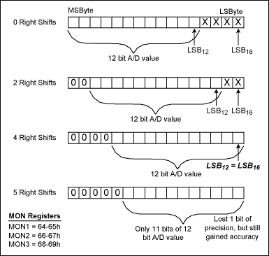
Figure 3. MON register right-shifting examples. How to Calibrate InternallyWhile there are several ways internal calibration can be performed, this application note focuses on the binary-search approach described in the DS1856 data sheet. The outputs of the pseudo-code algorithm are scale (gain) and offset register values, which yield the desired transfer function (the desired LSB).
To use the pseudo-code algorithm, the laser must be set to two different intensities. One setting is a minimum intensity setting and the other is 90% of the maximum intensity. The ability to switch back and forth between the two settings must be available . For non-optical applications, two different voltages must be applied to the MON inputs. The algorithm provided in the data sheet uses 90% of the maximum possible input voltage so that the upper limit is less likely to clamp. When using a percentage of the desired full scale as the maximum value, however, it is important to calculate the corresponding percentage of the digital values ​​as well.
The algorithm begins by setting both the Offset and Right-Shifting registers to 0000h. Next, the binary search for the scale (gain) value is initiated by setting the Scale Cal register to half scale, 8000h. The gain is then tested by applying the 90% maximum input to the MON channel being calibrated, and then reading the corresponding digital conversion. This value is then called Meas2. Meas2 is checked to see if it is clamped at FFF8h. If the reading is clamped, one cannot conclude whether the conversion is actually FFF8h or if it is greater than that, but just clamped to FFF8h. Because the result is too high, the next step in the binary search is to cut the gain value in half; the 90% maximum input is again applied to check for clamping. The process repeats until a non-clamping gain value is found.
As soon as a non-clamping Meas2 is found, the algorithm continues by forcing the null input and reading its digital conversion value. This value becomes Meas1. The values ​​CNT1 (null / LSB) and CNT2 (90% of full-scale value / LSB) are the calculated desired-conversion output values. The delta between Meas2 and Meas1 is calculated and compared to the desired delta (CNT2-CNT1) using the constants calculated at the beginning of the algorithm. If Meas2-Meas1 is less than CNT2- CNT1, then the gain is again cut in half. However, if Meas2-Meas1 is greater than CNT2-CNT1, then the gain is increased by cutting the gain in half and adding it to the current gain value. The process repeats until a total of 16 iterations are performed. The resultant is a 16-bit value that yields the desired gain (and desired LSB).
There is an alternate way of visualizing the gain calibration procedure. Beginning with the MSB (b15) of the 16-bit Scale Cal register, set the bit to a 1 (all other bits are initially set to 0). With the MSB = 1 , the process of applying the analog input and reading the digital output is performed. If the digital output is clamped, then the gain is too high and the MSB is written back to a 0. Otherwise, the MSB remains a 1.The MSB is now known. Next, with b15 set to what was already determined, set b14 to 1 and leave b13 through b0 set to 0. Go through the process again to determine if the gain is still too high. If so, then b14 becomes a 0 Otherwise, it becomes a 1. The procedure continues until all 16 bits are determined. The result is again a 16-bit value which yields the desired gain.
Once the desired gain is determined, a new offset can be calibrated or it can be left at 0000h (no offset). The calibration method depends on how the offset feature is to be used. The explanation accompanying the algorithm in the data sheet assumes that the user wants to apply a negative offset to null out the digital readings, so that a null input on the MON pin will produce all zeros on the digital output. This is achieved by applying the null input on the calibrated MON input and reading the conversion . For example, if the null input produces a digital output of 20h, then the offset can be programmed so that 20h will be digitally subtracted from every conversion. In this example, 20h is substituted into the offset formula and the result is then programmed into the Offset Cal register for the desired MON channel. Internal Calibration And Right-Shifting ExampleAnother example presented here demonstrates the concepts presented in this application note. In this example, MON3 is used to monitor RxPower. When the minimum input of -40dBm is applied, a voltage of 10mV is presented to the MON3 pin of the DS1856. The desired digital output for this input is 0000h. When a 0dBm signal is applied, 300mV is present on MON3. The desired digital output in this case is 2710h and was chosen to satisfy the LSB dictated by SFF-8472. (The LSB for RxPower is 0.1µW.)
The next step is to determine the ideal number of right shifts. As the range of the desired digital output is 0000h to 2710h, Table 9 of the DS1856 data sheet can be used to select the ideal number of right shifts, which is 2 in this case.
To achieve a final digital output of 2710h after the two right shifts, we must set the Scale Cal value so that a 300mV input results in a conversion of 9C40h (2710h times 22) before the right shifts occur. Therefore, internal calibration will be used to calculate the gain so that the ADC will produce a conversion to 9C40h for an input of 300mV. Once the internal calibration and programming of the offset are complete, two right shifts will be enabled. Our example is summarized in Table 2.
Table 2. Internal Calibration And Right-Shifting Example
| Customer Signal Rx Power (dBm) | Voltage Applied to MON3 Pin (mV) | Digital Outputs During Cal (0 right shifts) | Final Digital Output (Two Right Shifts) |
| -40 | 10 | 0000h | 0000h |
| 50 | 0563h | ||
| 100 | 0C1Fh | ||
| 150 | 12DBh | ||
| 200 | 1997h | ||
| 250 | 2051h | ||
| 0 | 300 | 9C40h | 2710h |
Once the relationship between input and output is determined (shown in Table 2), the internal calibration routine provided in the DS1856 data sheet is used to internally calibrate the device. The routine begins by performing some preliminary calculations, as shown below. Notice that the 90% shown in the data sheet routine is not used here because the second calibration point (300mV = 9C40h) is already less than 90% of the full-scale value. As a result, the internal calibration routine used in this example has all references to the 90% removed.
Given Table 2, the following calculations are made: LSB = (0.300V-0.010V) / (9C40h-0000h) = 0.290V / 40,000 = 7.25µV
Full-Scale Voltage = FS = LSB x 65535 = 7.25µV x 65535 = 0.475128V
CNT1 = 0.010 / LSB = 1379.3 => 1379 (dec)
CNT2 = 0.300 / LSB = 41379.31 => 41379 (dec) CNT1 and CNT2 are the expected (desired) digital outputs when the two calibration points are applied. The internal calibration routine will result in a slope as close as possible to the slope determined by these two values.
The iterative portion of the routine goes through 16 cycles of programming a slope in a binary search fashion, and then compares to see if it is equivalent to the desired slope. For this example, a DS1856 was calibrated using the internal calibration procedure and the inputs and outputs of all 16 iterations are shown in Table 3.
The first column of Table 3, Iteration, is equivalent to n in the routine. The column gain_result is the value programmed into the Scale Cal register (device Table 03h, bytes 98-99h) for every iteration. Columns Meas2 and Meas1 are the digital values ​​read from the device with 300mV and 10mV applied to the input, respectively. Finally, for iterations in which Meas2 did not clamp, Meas2-Meas1 is compared to CNT2 -CNT1. If Meas2-Meas1 is greater than CNT2-CNT1, then the gain_result is too large. The Scale Cal bit corresponding to that iteration becomes a zero, which in turn determines the gain_result of the successive iteration. Once all 16 iterations are complete, the Scale Cal value is known. The device used in this example resulted in a Scale Cal value of 5038h.
Table 3. Internal Calibration Values
| Iteration | gain_result | Meas2 | Meas1 | Meas2 | Meas1 | Meas2-Meas1 | CNT2-CNT1 | bit result | Scale Cal |
| (dec) | (hex) | (hex) | (dec) | (dec) | (dec) | (bin) | (hex) | ||
| 15 | 8000 | FD58 | 0870 | 64856 | 2160 | 62696 | 40000 | 0 | 5 |
| 14 | 4000 | S2A0 | 0450 | 33440 | 1104 | 32336 | 40000 | 1 | |
| 13 | 6000 | C010 | 0658 | 49168 | 1624 | 47544 | 40000 | 0 | |
| 12 | 5000 | A138 | 0558 | 41272 | 1368 | 39904 | 40000 | 1 | |
| 11 | 5800 | B0BS | 0500 | 45240 | 1280 | 43960 | 40000 | 0 | 0 |
| 10 | 5400 | A938 | 05A0 | 43320 | 1440 | 41880 | 40000 | 0 | |
| 9 | 5200 | A530 | 0578 | 42288 | 1400 | 40888 | 40000 | 0 | |
| 8 | 5100 | A328 | 0568 | 41768 | 1384 | 40384 | 40000 | 0 | |
| 7 | 5080 | A238 | 0568 | 41528 | 1384 | 40144 | 40000 | 0 | 3 |
| 6 | 5040 | A1A8 | 0560 | 41384 | 1376 | 40008 | 40000 | 0 | |
| 5 | 5020 | A170 | 0558 | 41328 | 1368 | 39960 | 40000 | 1 | |
| 4 | 5030 | A190 | 0558 | 41360 | 1368 | 39992 | 40000 | 1 | |
| 3 | 5038 | A198 | 0558 | 41368 | 1368 | 40000 | 40000 | 1 | 8 |
| 2 | 503C | A1A0 | 0558 | 41376 | 1368 | 40008 | 40000 | 0 | |
| 1 | 503A | A1A0 | 0558 | 41376 | 1368 | 40008 | 40000 | 0 | |
| 0 | 5039 | A1A0 | 0558 | 41376 | 1368 | 40008 | 40000 | 0 | |
With the device programmed to its new Scale Cal value, the Offset Cal is determined by forcing 10mV (the voltage at which we want to read 0000h) and reading the digital result. The device used in this example produced a value of 0558h with 10mV applied . Using the offset formula, the Offset Cal is calculated as:
MON3 Offset Cal = [0558h / 4] = 0156h
The value 0156h is written to the MON3 Offset Cal register bytes.
The new clamp value can be calculated as follows:
New clamp value (pre-right shift) = FFF8h-0558h = FAA0h
With the internal calibration complete, the two right shifts are enabled by writing 20h to Table 03h, location 8Fh. ConclusionThe internal calibration and right-shifting features of the DS1856 provide the utmost flexibility and make the DS1856 suitable for a wide variety of applications. This application note provides additional information not found in the DS1856 data sheet, specifically why internal calibration and right shifting are beneficial as well as how to implement them. An example was also provided to tie the concepts together.
Questions / comments / suggestions concerning this application note can be sent t var name = "MixedSignal.Apps @"; var domain = "dalsemi.com"; document.write ("" + name + domain + ""); MixedSignal ..
Phlizon`s COB series Grow Light emits all the wavelengths of light which can be fully absorbed by the plants to create.
Best full Specturm designed to perfectly match large areas of indooor plants, especially for Medical Plant.
COB + Dual-chip,most efficient spectrum,high PPFD.Two cooling fans with double ball(import from Japan) and big aluminum heat sink to protect the grow lights from high temperature,good cooling,long lifespan.Photosynthesis and promote healthy growth budding and flowering.
1000w/2000w /3000w Cob Led Grow Light, it will give you more options when your plants need different strength of illumination.
Grow Lights are a great choice for growers who are dealing with hot HPS lights and want to change to something that's going to run cooler. Although Led Grow Lights do produce heat,the smaller models might not bring up the temperature of your grow space.Even the more powerful models of LED Grow Lights that produce a lot of heat still have built-in cooling systems to help prevent the heat from beaming directly down onto your plants.
3000w Led Grow Light Features
Indoor grow light
COB series, high power branded CREE COB with high Par value and deeper penetration
VEG/BLOOM and STRONGER switches for each grow stage.
Special spectrum for plant growing to increase the yield.
Building to Harvest: Beneficial for seeding to fruiting stage.
Good quality fans with low noise.
Easy to install by minute
Energy Saving, environmental friendly
3 Years Warranty
Compare led grow light to traditional HPS/MH grow light

WHAT MAKE UP AN EXCELLENT LED GROW LIGHT ?
1.PPFD Value : PPFD is Photosynthetic Photon Flux Density. When you choose a plant light, you should compare the PPFD values of different plant lights. The larger the value, the better the growth of the plant.
2.Actual Power: Because the actual power of the plant light always varies with different conditions, all Amazon sellers use the rated power to describe the power of the product because the rated power is constant. When you pick a LED grow light, the rated power of the plant light is a reference, and more importantly is the actual power.
3.Core Coverage: In addition to the above two, when you choose a plant light, you also need to compare the cover area of different plant lights, of course, the size of the core coverage area. In general, in germination stage, you can hang the plant light higher and the cover area is larger. In flowering stage you can hang the plant light lower and the cover area is smaller because the plant needs more light at this stage. You have to compare different coverage areas to choose the plant light that suits you.

Detailed images of 1000w 2000w 3000w 400w COB LED Grow Light


Applications
Hydroponics, Horticulture, Agriculture and Greenhouse
Locations: Farm, Exhibition, Garden, Home, Urban, Bonsai, and University Lab
Growth of Fruits, Vegetables, Flowers and so on
Seeding, Rooting, Breeding, Flowering and Fruiting period

Packaging and Shipping

2. By Air or by Sea for batch goods, for FCL; Airport/ Port receiving;
3. Customers specifying freight forwarders or negotiable shipping methods!
4. Delivery Time: stock avaiable sample will be delivered immediately ; 3-7 days for trial order; 7- 25 days for batch goods
Suggestions:
1.Clean the dust inside every 6 months to ensure the good heat dissipation and long life time.
2.Don`t keep too short distance to the plant canopy to avert leaves bleaching.
3. Highly hang the lamp will weaken the energy and affect the growth cycle of the plants, so the lamp should not be hang too high.
4. While taking care of the plants, please spray the leaves and branches 2-3 times everyday, to ensure the plants do not wrinkle a wither, and have no phenomenon of few fruit, and hard pericarp
Trade Terms
Payment: T/T, L/C, Paypal, 30% deposits before production, 70% balance to be paid before deliverying(Western Union are welcome)
Sample will be delivered within 7 working days.
Discounts are offered based on order quanlityes.
MOQ:sample order are acceptable
Delivery ways:DHL,UPS,FedEx,TNT, door to door,by sea,by air,etc.
PHLIZON LOOKING FOR DISTRIBUTOR ALL OVER THE WORLD
If you are interested in, and
1.own several store for agriculture in your local market
2.or in the business of grow light equipment
3.or good relationship with grower or greenhouse owner
To be a distributor, max support will be offered:
1.price support
2.technical support
3.new product support
4.24 hours after-sales service online
PH-B-L6
Optic Cree Cob Grow Light,600W Led Indoor Grow Lights,630W Led Grow Light,Cob 3000W Grow Light
Shenzhen Phlizon Technology Co.,Ltd. , https://www.philizon.com