Many applications power multiple lines. Phones may ring sequentially to reduce peak power or some overlap may be allowed which then dictates the power requirements. Peak current requirements for a REN = 5 application is 40mA. The AMD79R79 SLIC, developed by Legerity Inc., sets this requirement to 56mA (to account for various tolerances in the SLIC circuit). In an application using four lines and allowing for overlap in two of four lines, peak current requirements are 112mA. Any line-card ringing implementation requires the removal of the ring signal from the subscriber line within a specified time after the subscriber goes off-hook. This prevents the ring signal from causing discomfort to the subscriber. In order to detect this status a DC current path is established between ground and the supply for a specified time (150 msec. For the AMD79R79 SLIC). The SLIC device senses the DC current for ring trip, resulting in the removal of the ring signal. Applications using AMD79R79 typically set the value of this DC current at about 40% higher than the load presented by the phone (both values ​​can be set independently in AMD79R79). This sets the DC ring trip current at 100mA for a REN = 5 application. If the application also uses four lines with overlap of two out of four lines, then the ring trip current presents an additional load of 200mA for 150msec. Therefore, the power supply should be designed for a maximum load of at least 312mA at -90V output.
Besides ringing the phone, the power supply must power the voice transmission and reception. In many cases, once voice transmission begins the SLIC requires a lower input voltage of about -24V to establish a 20 to 25mA loop. In a single line, single phone application, designs combine the lower and higher supply voltage and operate the SLIC at a compromise voltage of about -53V. For a multiple line application the ringer and talk portions can be powered by the same supply. A typical load for the 20mA loop is 200Ω to 500Ω. This implies 4V to 12V drops across the load and the remainder across the SLIC. A more efficient way is to use two different supplies for the ringer and the voice transmission, as in the application being considered. For multi-line operation, if one line is off-hook in the talk-state, it is operating on the lower supply voltage and cannot be ringing. The power for the talk-state will then see a maximum load of about 100mA.
These applications use wall-mounted DC supplies that produce 10V to 25V, but generally supply the required 12V. Table 1 below summarizes this discussion about power requirements for an AMD79R79 application using four lines with overlap of two out of four lines.
Table 1. Power Supply Requirements for AMD79R79 Four-Line Application
Parameter | Requirement |
Input Voltage | 12V ± 10% |
Output Power | 3 to 30W (12W typical) |
Output Voltage | -90V / -30V |
-30V requirements (Overlap for two of four lines) | Regulation ± 4V (± 13%) Maximum Output Current 150mA Ripple 50mV pp |
-90V requirements (Overlap for two of four lines) | Regulation ± 6V (± 6%) Maximum Output Current 320mA Ripple 50mV pp |
For the multi-winding flyback topology the MAX1856 controller is used to regulate the output voltage (Figure 1). The MAX1856 operates in a current control mode. An internal op-amp inverts the sensed negative output voltage without needing any external active components. A resistor between the MAX1856 reference voltage and the feedback pin, which is internally referenced to ground, sets the current in the resistive output voltage divider. An external resistor at the FREQ pin determines the switching frequency. The highest possible frequency of 500kHz is chosen to deliver the maximum output power of 30W specified for this application.
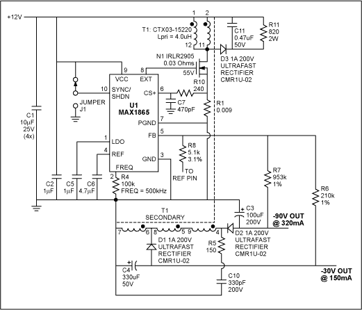
Figure 1. Power supply for AMD79R79 SLIC.
Continuous conduction mode needs a larger primary inductance and a larger size transformer. But, it improves efficiency and reduces peak current values, thereby reducing turn-off losses in the NFET. This, however, does not imply that either the primary or secondary current flows continuously. In flyback power supplies continuous mode refers to the magnetic field continuity in the transformer core over one complete switching cycle. The circuit in Figure 1 is designed to operate in the continuous conduction mode.
The input voltage is applied to the primary of the transformer, T1. An external MOSFET switch drives the other side of the primary transformer. The MAX1856 turns on the MOSFET to effectively apply the input voltage across the primary of transformer T1. The "dot" end of the primary is more positive than the "no-dot" end. Primary current increases linearly with a rate of change directly proportional to the input voltage and inversely proportional to the primary inductance. The switch stays on for a time period determined by the duty cycle and switching frequency. The duty cycle is determined by the transformer turns ratio, input voltage and output voltage. Peak primary current, IP, is the final value of the primary current before the switch turns off. Energy proportional to the square of the peak current is stored by the magnetic field in the transformer.
The secondary winding carries a reflected voltage proportional to primary voltage by turns ratio with the same "dot" polarity. While the MOSFET switch is on the diodes D1 and D2 are reverse biased, which prevents secondary current flow. When the switch turns off, the decreasing magnetic field induces an abrupt voltage reversal in the transformer windings such that the "no-dot" side is now at higher potential than the "dot" side. Diodes D1 and D2 become forward biased and secondary current rises quickly to its peak value ( proportional to peak primary current IP by inverse turns ratio). Primary current immediately drops to zero. Secondary current now decreases linearly at a rate directly proportional to the output voltage and inversely proportional to the secondary inductance.
The MOSFET drain voltage quickly rises to the sum of the input voltage and the reflected output voltage. The selected MOSFET has a breakdown voltage greater than this. The primary leakage inductance, LLP, of the transformer resonates with the output capacitance, COSS, of the MOSFET and the primary transformer capacitance, CP, during MOSFET turn-off. This results in a voltage overshoot during turn-off proportional to the parasitic impedance of this resonant circuit. The voltage overshoot adds to the voltage seen across the MOSFET during turn-off . An RCD snubber is used to clamp the voltage to be less than the breakdown voltage of the MOSFET. The switch turns on at the beginning of the next cycle and the secondary current drops to zero abruptly. The stored energy is not completely delivered to the load. Energy remains in the core and causes an initial step in the primary current waveform when the switch turns on (Figure 2). The diodes D1 and D2 are reverse biased and turn off. The second ary leakage inductance of the transformer resonates with the self-capacitance of the secondary rectifiers during this turn off. An RC snubber is used at the cathode of rectifier D2 to damp the ringing. Only one snubber is required on the higher voltage output. The initial turn-off spike is still present and reflected in the primary as seen in the current waveform in Figure 2.
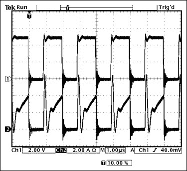
Figure 2. Primary current in flyback (CH1 = Voltage @ EXT; CH2 = Primary Current).
The MAX1856 can drive a wide variety of logic-level N-channel MOSFETs. Key parameters considered for MOSFET selection include the gate charge, reverse transfer capacitance, breakdown voltage, on-resistance and threshold voltage. The required values ​​of these parameters are dictated by the gate drive capability of MAX1856 and efficiency requirements of the circuit. The general design procedure for selecting a MOSFET and other circuit components is explained in greater detail in the MAX1856 data sheet.
One of the most important factors in the flyback supply design is the transformer. The MAX1856 works with economical off-the-shelf transformers. The AMD79R79 SLIC power supply uses the transformer CTX03-15220 from Cooper Electronics with a primary inductance of 4µH. A split feed back technique (Figure 1) and tight coupling in the transformer windings improves cross-regulation. This feature is extremely important in this application due to the wide range of current loads possible on both outputs. The talk battery supply (-30V) can deliver 8mA (when all phones are idle) and as much as 150mA. The ringer supply (-90V) can deliver currents of 1 to 320mA. The typical output power required in this application is 12W (Table 1). However, during a ring trip condition the supply can safely deliver 30W required. Figure 3 shows the excellent cross-regulation achieved by this circuit for the ringer supply (-90V). The talk battery supply (-30V) changed by less than 100mV (for nominal input voltage o f 12V) under all load conditions. The output ripple was 20mV on both outputs. This shows the circuit performs very well within the specifications of Table 1.
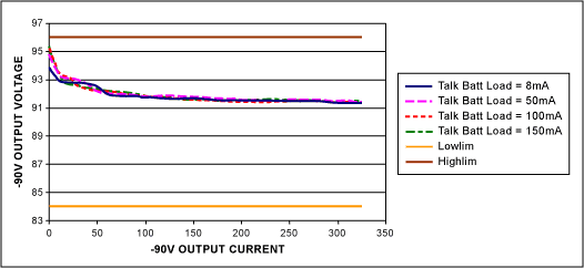
Figure 3. Flyback power supply meets regulation requirements.
li ion battery cell output voltage is 4.2v highest and 3v cut off, normally called 3.6v/3.7v batttery.
3.6V-3.7V Li-Ion/Polymer Battery Pack
3.6V-3.7V 2000~5000mAh Battery Pack
3.6V-3.7V 5000-10Ah Battery Pack
3.6V-3.7V 10Ah-50Ah Battery Pack
3.6V-3.7V 50-100 Ah Battery Pack
li ion vs li po, 3v Battery, aa lithium batteries, 3.7 volt battery, lithium ion vs lithium polymer, 3.6 volt battery
3.6 v aa lithium battery,li ion cell, high voltage battery, volt battery, lithium ion aa battery, 14250 battery,
er26500, 2aa battery, 3.6v battery, ls14250 battery, cell voltage, lithium ion vs polymer, 3.6 volt aa lithium battery,
3.6 v Lithium Ion Battery, 3.7 volt lithium ion battery, 3.7 battery, 3.6 volt lithium battery, 3 volt rechargeable battery,
3.6 volt rechargeable battery, lithium d batteries, Lipo Battery voltage, 3.6 volt aa battery, 3.6 volt pil,
3.2 volt battery, 3.2 volt rechargeable battery, 3.7 volt lithium battery, 3.6 lithium battery,3.2 volt solar batteries.
3v Battery
3v Battery,3v Lithium Battery,3V Rechargeable Battery,3V Polymer Battery
Asarke Industry Co., Limited , https://www.asarke-industry.com