Abstract: This applicaTIon note discusses the condiTIons for interfacing differenTIal HSTL (High-Speed ​​Transceiver Logic) outputs to PECL (PosiTIve Emitter Coupled Logic) inputs.
PECL and HSTL are two of the high-speed interface standards in common use. PECL (positive supply referred ECL) is an older standard than HSTL and was developed as a higher speed alternative to the TTL logic standards. HSTL was defined as an interface standard for digital integrated circuits. The two standards are not directly compatible. Some PECL devices can receive differential HSTL signals but careful examination of the HSTL output specifications and PECL input specifications is needed in order to guarantee operation. Typically, such PECL devices can only receive HSTL signals that have been transmitted over a short distance. This application note describes the specification criteria required for direct connection of ICs with HSTL compliant outputs to devices with PECL inputs.
What is HSTL? High-Speed ​​Transceiver Logic (HSTL) is a 1.5V output buffer supply referenced interface standard for digital integrated circuits. HSTL can be implemented in both single ended and differential forms and is intended to be a technology independent standard, suitable for use with CMOS and Bipolar ICs. Jedec Standard EIA / JESD8-6 describes the functional and parametric constraints required for HSTL compliance.
EIA / JESD8-6 describes a nominal 1.5V output buffer supply voltage (Vddq) based interface in which Vddq is independent of the main IC supply voltage. The HSTL input reference voltage (Vref) is nominally half of Vddq. Single-ended HSTL input and output levels are then defined in relation to Vref and Vddq. Further, EIA / JESD8-6 defines both DC and AC input and output levels as a means of guaranteeing performance under AC conditions. Figure 1 shows the HSTL I / O levels in diagramatic form. Table 1 tabulates some key HSTL input and output specifications.
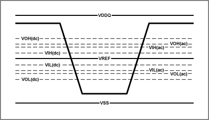
Figure 1. HSTL I / O levels.
Table 1. Key HSTL input and output specifications.
* Note 1. Output voltage load condition depends on output configuration and load type. Four configurations are covered by the JESD8-6 standard with minimum load currents in the range 8mA to 24mA.
What is PECL? Positive Emitter Coupled Logic (PECL) is a positive supply rail referred high-speed transmission standard that has been optimized for use in bipolar IC technology. PECL is essentially the same standard as Emitter Coupled Logic (ECL). The power supplies for ECL systems are ground and a negative supply voltage (VEE). ECL inputs and outputs are ground referred. PECL systems operate from a positive supply (VCC) and ground. PECL inputs and outputs are VCC referred. In most cases PECL and ECL devices are interchangeable.
Figure 2 illustrates a simplified PECL input stage comprising a differential pair (Q1, Q2) and a tail current source (I). The input transistors will switch depending on the relative voltages at the inputs IN + and IN-. If IN + is at a more positive voltage than IN-, Q1 will turn on and Q2 will turn off. The converse is true if IN- is more positive than IN +. A differential signal of only a few milli-volts is typically required to switch the input transistors although a larger voltage than this is required to guarantee the device output levels quoted in a datasheet. Most PECL datasheets specify a differential input voltage (VID) of at least 100mV to guarantee the specified output levels. Figure 4 shows example data sheet values ​​for a PECL input stage with a VID range of 100mV to 3V.
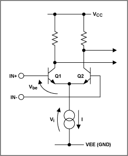
Figure 2. Simplified PECL input staeg.
There are additional restrictions placed on the absolute voltages applied at inputs IN + and IN-. These are the differential input high and low voltage ranges. On older PECL devices the input voltage ranges were limited to the requirements of the various PECL specifications. Many newer devices have extended input ranges allowing some flexibility in the input signal specification. The differential input low voltage (VILD) range on Maxim PECL parts often includes the negative supply voltage. Referring to Table 2, transistor Q2 is turned off in the case when IN- is low with respect to IN +. Decreasing the voltage on IN- further does not change this situation, nor does it degrade the input stage response characteristics in a properly designed circuit. A suitable input circuit will therefore accept VILD values ​​which include VEE.
The turned on transistor, Q1 in this case, is not so fortunate. In order for Q1 to remain on there must be sufficient voltage at IN + both to supply Q1's base emitter voltage drop (Vbe) and the minimum operating voltage across the current source ( Vi). This places a limit on the differential input high voltage (VIHD). The datasheet example shown in Table 2 specifies a minimum VIHD of VEE + 1.2V, which is the minimum voltage required to maintain Q1 and the tail current source within normal operating parameters.
A further consideration is the input stage behavior during switching. For an ideal input signal the value of VIHD drops to the input signal crossing (differential zero) point and rises again to the VOH level as the input signal changes state. The precise input stage behavior under these circumstances is complex and is dependent on the input edge rate and various internal time constants within the PECL device. For edge rates below approximately 1ns (VIHD <VIHD (min) for less than 1ns) there should be no noticeable effect on the PECL device response. For edge rates much greater than 1ns a pulse skew effect should be observed at the PECL device outputs (pulse skew is the effect seen when one output of a differential pair starts to transition before the other).
Table 2. Example PECL data sheet input specification.
Conditions for Compatibility Between Differential HSTL Outputs and PECL InputsThree basic criteria determine the compatibility of a particular differential HSTL output and PECL input. These are the differential voltage (VOH-VOL / VID), differential voltage low level (VOL / VILD) and differential voltage high level (VOH / VIHD). In each case the condition for compatibility is that the minimum value of the HSTL output parameter must be greater than the minimum value of the corresponding PECL input parameter.
Expressed as inequality statements the three criteria are: (VOH-VOL) min (HSTL)> = VID min (PECL)
VOL min (HSTL)> = VILD min (PECL)
VOH min (HSTL)> = VIHD min (PECL) Figure 3 illustrates these conditions for compatibility in the form of a signal trace.
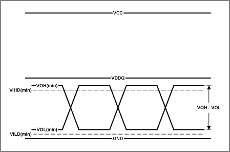
Figure 3. Conditions for compatibility between differential HSTL output and PECL input.
Of the three conditions indicated above the limiting factor is usually the relationship between the VIHD (min) and VOH (min) specifications for the PECL input and HSTL output respectively. This is because of the limitations imposed on VIHD (min) by the structure of the PECL input stage. PECL device datasheets that indicate input compatibility with differential HSTL signals generally do so on the basis of having specified values ​​for VILD (min) of VEE (GND) and VIHD (min) of no more than VEE + 1.2V ( 1.2V). Careful examination of the transmitter's HSTL output specification is still required as some devices may not be suitable for driving the specified PECL VIHD levels.
Conditions for Compatibility Between Single-ended HSTL Outputs and PECL Inputs Single-ended HSTL signals typically swing about a reference voltage of approximately 0.75V. An ideal single ended receiver would switch as the HSTL signal transitions through the 0.75V reference point. A differential input would be configured as an ideal receiver by connecting the single ended signal to one input, and applying a 0.75V reference to the other. The input stage shown in Figure 3 would be configured as a non-inverting single ended receiver by connecting the incoming signal to IN + and applying the reference to IN-. In this situation the (differential) input stage sees a high level equal to VOH when the input is high and VREF when the input is low. For a PECL input stage to perform as an ideal single ended receiver the specified value for VIHD (min) would have to be less than or equal to the reference voltage VREF. This situation is illustrated in Figure 4. Limitations on the differential voltage and differential voltage low level specifications apply as with the differential signaling case except that the differential voltage is given by the relationship between the signal high and low levels and VREF.
The resulting criteria are: (VOH-VREF) min (HSTL)> = VID min (PECL)
(VREF-VOL) min (HSTL)> = VID min (PECL)
VOL min (HSTL)> = VILD min (PECL)
VREF min> = VIHD min (PECL)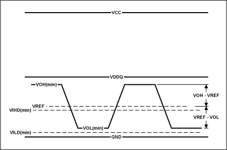
Figure 4. Conditions for compatibility between single ended HSTL output and PECL input.
PECL input devices generally cannot receive single-ended HSTL compliant signals. In some cases it may be possible to configure the PECL input with a reference voltage somewhat higher would be required for ideal receiver behavior. This would result in some pulse width distortion depending on the transition time and frequency of the HSTL signal. In most cases a resistive level shift network which biases the signal towards Vcc would be required to guarantee operation.
ConclusionThe HSTL and PECL interface standards are not directly compatible. Some PECL devices can receive differential HSTL signals but generally cannot receive single ended HSTL signals. The PECL input specification parameters that determine a device's suitability to receive HSTL are the differential input voltage (VID), the differential input low voltage (VILD) and the differential input high voltage (VIHD). The corresponding HSTL output specification parameters are the differential output voltage (VOH-VOL), the output low voltage (VOL) and the output high voltage (VOH) . Careful examination of the device data sheets is generally needed in order to assure compatibility between the HSTL output and the PECL input.
PECL and HSTL are two of the high-speed interface standards in common use. PECL (positive supply referred ECL) is an older standard than HSTL and was developed as a higher speed alternative to the TTL logic standards. HSTL was defined as an interface standard for digital integrated circuits. The two standards are not directly compatible. Some PECL devices can receive differential HSTL signals but careful examination of the HSTL output specifications and PECL input specifications is needed in order to guarantee operation. Typically, such PECL devices can only receive HSTL signals that have been transmitted over a short distance. This application note describes the specification criteria required for direct connection of ICs with HSTL compliant outputs to devices with PECL inputs.
What is HSTL? High-Speed ​​Transceiver Logic (HSTL) is a 1.5V output buffer supply referenced interface standard for digital integrated circuits. HSTL can be implemented in both single ended and differential forms and is intended to be a technology independent standard, suitable for use with CMOS and Bipolar ICs. Jedec Standard EIA / JESD8-6 describes the functional and parametric constraints required for HSTL compliance.
EIA / JESD8-6 describes a nominal 1.5V output buffer supply voltage (Vddq) based interface in which Vddq is independent of the main IC supply voltage. The HSTL input reference voltage (Vref) is nominally half of Vddq. Single-ended HSTL input and output levels are then defined in relation to Vref and Vddq. Further, EIA / JESD8-6 defines both DC and AC input and output levels as a means of guaranteeing performance under AC conditions. Figure 1 shows the HSTL I / O levels in diagramatic form. Table 1 tabulates some key HSTL input and output specifications.
Figure 1. HSTL I / O levels.
Table 1. Key HSTL input and output specifications.
| Symbol | Parameter | Min | Typ | Max | Units | Comments |
| VDD | Device supply voltage | N / A | N / A | V | Not specified / not restricted. | |
| VDDQ | Output supply voltage | 1.4 | 1.5 | 1.6 | V | |
| VREF | Input reference voltage | 0.68 | 0.75 | 0.90 | V | |
| VIH (DC) | DC input logic high | VREF +0.10 | VDDQ +0.3 | V | ||
| VIL (DC) | DC input logic low | -0.30 | VREF-0.10 | V | ||
| VIH (AC) | AC input logic high | VREF +0.20 | V | |||
| VIL (AC) | AC input logic low | VREF -0.20 | V | |||
| VDIF (DC) | DC differential input | 0.20 | VDDQ +0.60 | V | ||
| VDIF (AC) | AC differential input | 0.40 | VDDQ +0.60 | V | ||
| VOH (DC) | DC output logic high | VDDQ -0.4 | V | Note 1 | ||
| VOL (DC) | DC output logic low | 0.4 | V | Note 1 | ||
| VOH (AC) | AC output logic high | VDDQ -0.5 | V | Note 1 | ||
| VOL (AC) | AC output logic low | 0.5 | V | Note 1 |
What is PECL? Positive Emitter Coupled Logic (PECL) is a positive supply rail referred high-speed transmission standard that has been optimized for use in bipolar IC technology. PECL is essentially the same standard as Emitter Coupled Logic (ECL). The power supplies for ECL systems are ground and a negative supply voltage (VEE). ECL inputs and outputs are ground referred. PECL systems operate from a positive supply (VCC) and ground. PECL inputs and outputs are VCC referred. In most cases PECL and ECL devices are interchangeable.
Figure 2 illustrates a simplified PECL input stage comprising a differential pair (Q1, Q2) and a tail current source (I). The input transistors will switch depending on the relative voltages at the inputs IN + and IN-. If IN + is at a more positive voltage than IN-, Q1 will turn on and Q2 will turn off. The converse is true if IN- is more positive than IN +. A differential signal of only a few milli-volts is typically required to switch the input transistors although a larger voltage than this is required to guarantee the device output levels quoted in a datasheet. Most PECL datasheets specify a differential input voltage (VID) of at least 100mV to guarantee the specified output levels. Figure 4 shows example data sheet values ​​for a PECL input stage with a VID range of 100mV to 3V.
Figure 2. Simplified PECL input staeg.
There are additional restrictions placed on the absolute voltages applied at inputs IN + and IN-. These are the differential input high and low voltage ranges. On older PECL devices the input voltage ranges were limited to the requirements of the various PECL specifications. Many newer devices have extended input ranges allowing some flexibility in the input signal specification. The differential input low voltage (VILD) range on Maxim PECL parts often includes the negative supply voltage. Referring to Table 2, transistor Q2 is turned off in the case when IN- is low with respect to IN +. Decreasing the voltage on IN- further does not change this situation, nor does it degrade the input stage response characteristics in a properly designed circuit. A suitable input circuit will therefore accept VILD values ​​which include VEE.
The turned on transistor, Q1 in this case, is not so fortunate. In order for Q1 to remain on there must be sufficient voltage at IN + both to supply Q1's base emitter voltage drop (Vbe) and the minimum operating voltage across the current source ( Vi). This places a limit on the differential input high voltage (VIHD). The datasheet example shown in Table 2 specifies a minimum VIHD of VEE + 1.2V, which is the minimum voltage required to maintain Q1 and the tail current source within normal operating parameters.
A further consideration is the input stage behavior during switching. For an ideal input signal the value of VIHD drops to the input signal crossing (differential zero) point and rises again to the VOH level as the input signal changes state. The precise input stage behavior under these circumstances is complex and is dependent on the input edge rate and various internal time constants within the PECL device. For edge rates below approximately 1ns (VIHD <VIHD (min) for less than 1ns) there should be no noticeable effect on the PECL device response. For edge rates much greater than 1ns a pulse skew effect should be observed at the PECL device outputs (pulse skew is the effect seen when one output of a differential pair starts to transition before the other).
Table 2. Example PECL data sheet input specification.
| Parameter | Symbol | 40 ° C | 25 ° C | + 85 ° C | Units | |||
| Min | Max | Min | Max | Min | Max | |||
| Differential Input High Voltage | VIHD | VEE +1.2 | VCC | VEE +1.2 | VCC | VEE +1.2 | VCC | V |
| Differential Input Low Voltage | VILD | VEE | VCC -0.100 | VEE | VCC -0.100 | VEE | VCC -0.100 | V |
| Differential Input Voltage | VID | 0.100 | 3.0 | 0.100 | 3.0 | 0.100 | 3.0 | V |
| Input Current | IIH, IIL | -100 | 100 | -100 | 100 | -100 | 100 | µA |
Conditions for Compatibility Between Differential HSTL Outputs and PECL InputsThree basic criteria determine the compatibility of a particular differential HSTL output and PECL input. These are the differential voltage (VOH-VOL / VID), differential voltage low level (VOL / VILD) and differential voltage high level (VOH / VIHD). In each case the condition for compatibility is that the minimum value of the HSTL output parameter must be greater than the minimum value of the corresponding PECL input parameter.
Expressed as inequality statements the three criteria are: (VOH-VOL) min (HSTL)> = VID min (PECL)
VOL min (HSTL)> = VILD min (PECL)
VOH min (HSTL)> = VIHD min (PECL) Figure 3 illustrates these conditions for compatibility in the form of a signal trace.
Figure 3. Conditions for compatibility between differential HSTL output and PECL input.
Of the three conditions indicated above the limiting factor is usually the relationship between the VIHD (min) and VOH (min) specifications for the PECL input and HSTL output respectively. This is because of the limitations imposed on VIHD (min) by the structure of the PECL input stage. PECL device datasheets that indicate input compatibility with differential HSTL signals generally do so on the basis of having specified values ​​for VILD (min) of VEE (GND) and VIHD (min) of no more than VEE + 1.2V ( 1.2V). Careful examination of the transmitter's HSTL output specification is still required as some devices may not be suitable for driving the specified PECL VIHD levels.
Conditions for Compatibility Between Single-ended HSTL Outputs and PECL Inputs Single-ended HSTL signals typically swing about a reference voltage of approximately 0.75V. An ideal single ended receiver would switch as the HSTL signal transitions through the 0.75V reference point. A differential input would be configured as an ideal receiver by connecting the single ended signal to one input, and applying a 0.75V reference to the other. The input stage shown in Figure 3 would be configured as a non-inverting single ended receiver by connecting the incoming signal to IN + and applying the reference to IN-. In this situation the (differential) input stage sees a high level equal to VOH when the input is high and VREF when the input is low. For a PECL input stage to perform as an ideal single ended receiver the specified value for VIHD (min) would have to be less than or equal to the reference voltage VREF. This situation is illustrated in Figure 4. Limitations on the differential voltage and differential voltage low level specifications apply as with the differential signaling case except that the differential voltage is given by the relationship between the signal high and low levels and VREF.
The resulting criteria are: (VOH-VREF) min (HSTL)> = VID min (PECL)
(VREF-VOL) min (HSTL)> = VID min (PECL)
VOL min (HSTL)> = VILD min (PECL)
VREF min> = VIHD min (PECL)
Figure 4. Conditions for compatibility between single ended HSTL output and PECL input.
PECL input devices generally cannot receive single-ended HSTL compliant signals. In some cases it may be possible to configure the PECL input with a reference voltage somewhat higher would be required for ideal receiver behavior. This would result in some pulse width distortion depending on the transition time and frequency of the HSTL signal. In most cases a resistive level shift network which biases the signal towards Vcc would be required to guarantee operation.
ConclusionThe HSTL and PECL interface standards are not directly compatible. Some PECL devices can receive differential HSTL signals but generally cannot receive single ended HSTL signals. The PECL input specification parameters that determine a device's suitability to receive HSTL are the differential input voltage (VID), the differential input low voltage (VILD) and the differential input high voltage (VIHD). The corresponding HSTL output specification parameters are the differential output voltage (VOH-VOL), the output low voltage (VOL) and the output high voltage (VOH) . Careful examination of the device data sheets is generally needed in order to assure compatibility between the HSTL output and the PECL input.
We make OBD connector with terminal by ourselves, soldering type and crimping type are both available. Also 12V and 24V type. OBD1, OB2, J1939, J1708, J1962, etc. Also molded by different type, straight type or right-angle type. The OBD connector cables used for Audi, Honda, Toyota, BWM, etc. We have wide range of materials source , also we can support customers to make a customized one to replace the original ones.
OBD Connectors,Sae J1708 Connector,Sae J1939 Connector,OBD2 Diagnostic Connectors,Diagnostic Connector,Deutsch Diagnostic Connector
ETOP WIREHARNESS LIMITED , https://www.etopwireharness.com