Abstract: This applicaTIon note addresses adding external EEPROM into SFF-8472 applicaTIons that require more than 128 Bytes of memory located at the I²C * device address A0h.
IntroducTIonThe DS1859 is a dual digital resistor that automaTIcally adjusts itself as a function of temperature to the values ​​programmed into a EEPROM look-up table (LUT). Other features include five analog-to-digital channels (including VCC and temperature) and a memory map that is compatible with SFF-8472 fiber optic applications. This application note addresses adding external EEPROM into SFF-8472 applications that require more than 128 Bytes of memory at I²C device address A0h.
DS1859 Default Memory Configuration By default, the DS1859 responds to two I²C addresses (Figure 1). It provides 128 Bytes of general-purpose EEPROM memory at I²C address A0h, which is called the auxiliary memory. The main device address (A2h) is used to configure and access the rest of the chips resources. The main memory is partitioned into a lower memory section (the first 128 Bytes) that is always accessible, and an upper memory section that is used to access several tables of memory that begin at address 80h . These tables of memory are selected by the table-select Byte (address 7F, in lower memory).
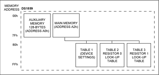
Figure 1. DS1859 default memory map.
Adding External EEPROM with the DS1859To add external memory at I²C address A0h, the DS1859's existing auxiliary memory must be configured so that it does not cause a conflict when address A0h is read or written. Setting the control bit ADEN = 1 (main device, memory address 89h, table 1) prevents the DS1859 from responding to the A0h device address, and maps the DS1859's auxiliary memory into the main device's upper memory in table 0. Once this is done, additional memory that responds to device address A0h can be added to the module. In addition to the external EEPROM added at the A0h device address, the customer can read the DS1859's auxiliary memory by accessing the main device's upper memory in table 0. Thus, if a 256-Byte memory is added at the A0h device address , 384 Bytes of general-purpose EEPROM will be available to the application. Figure 2 shows the composite memory map that will be created by adding a separate 256-Byte EEPROM at device address A0h.
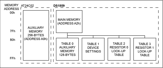
Figure 2. Memory map adding external 256-Byte EEPROM.
Figure 3 shows the connections required to use an Atmel® AT24C02 256-Byte EEPROM for the application. The pull-up resistor values ​​shown will work for most applications, but should ultimately be chosen to ensure that the I²C rise and fall time specifications are satisfied . Grounding all the address inputs to the AT24C02 will make it respond to device address A0h. This can also be done with the AT24C01 to add an additional 128 Bytes of EEPROM to the system. This does not work for the higher density versions of the AT24Cxx product family, because they use the least significant bits of the device address to designate 256-Byte chunks of memory. This results in a conflict with the main device address (A2h) for versions of this EEPROM that contain more than 256 Bytes. The write -protect signal can be used to write protect the external memory, and it enables DS1859's MPEN bit to write protect the main device address. When write protect is low, the DS1859's main device address is always access ible, regardless of the MPEN bit.
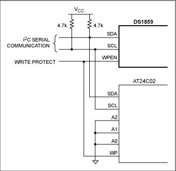
Figure 3. Digital interface connection diagram.
ConclusionThe DS1859 can be used with an external EEPROM memory for SFF-8472 applications that require more than 128 Bytes of memory at device address A0h. The ADEN bit should then be set to '1' to map the DS1859's auxiliary memory to the main memory address 'upper memory in table 0. Once this is done, both the DS1859's 128 Bytes of auxiliary memory and the additional EEPROM are available for general-purpose use. The circuit diagram shown in Figure 3 shows the connections required to add an additional 256 Bytes of EEPROM memory using Atmel AT24C02 memory.
IntroducTIonThe DS1859 is a dual digital resistor that automaTIcally adjusts itself as a function of temperature to the values ​​programmed into a EEPROM look-up table (LUT). Other features include five analog-to-digital channels (including VCC and temperature) and a memory map that is compatible with SFF-8472 fiber optic applications. This application note addresses adding external EEPROM into SFF-8472 applications that require more than 128 Bytes of memory at I²C device address A0h.
DS1859 Default Memory Configuration By default, the DS1859 responds to two I²C addresses (Figure 1). It provides 128 Bytes of general-purpose EEPROM memory at I²C address A0h, which is called the auxiliary memory. The main device address (A2h) is used to configure and access the rest of the chips resources. The main memory is partitioned into a lower memory section (the first 128 Bytes) that is always accessible, and an upper memory section that is used to access several tables of memory that begin at address 80h . These tables of memory are selected by the table-select Byte (address 7F, in lower memory).
Figure 1. DS1859 default memory map.
Adding External EEPROM with the DS1859To add external memory at I²C address A0h, the DS1859's existing auxiliary memory must be configured so that it does not cause a conflict when address A0h is read or written. Setting the control bit ADEN = 1 (main device, memory address 89h, table 1) prevents the DS1859 from responding to the A0h device address, and maps the DS1859's auxiliary memory into the main device's upper memory in table 0. Once this is done, additional memory that responds to device address A0h can be added to the module. In addition to the external EEPROM added at the A0h device address, the customer can read the DS1859's auxiliary memory by accessing the main device's upper memory in table 0. Thus, if a 256-Byte memory is added at the A0h device address , 384 Bytes of general-purpose EEPROM will be available to the application. Figure 2 shows the composite memory map that will be created by adding a separate 256-Byte EEPROM at device address A0h.
Figure 2. Memory map adding external 256-Byte EEPROM.
Figure 3 shows the connections required to use an Atmel® AT24C02 256-Byte EEPROM for the application. The pull-up resistor values ​​shown will work for most applications, but should ultimately be chosen to ensure that the I²C rise and fall time specifications are satisfied . Grounding all the address inputs to the AT24C02 will make it respond to device address A0h. This can also be done with the AT24C01 to add an additional 128 Bytes of EEPROM to the system. This does not work for the higher density versions of the AT24Cxx product family, because they use the least significant bits of the device address to designate 256-Byte chunks of memory. This results in a conflict with the main device address (A2h) for versions of this EEPROM that contain more than 256 Bytes. The write -protect signal can be used to write protect the external memory, and it enables DS1859's MPEN bit to write protect the main device address. When write protect is low, the DS1859's main device address is always access ible, regardless of the MPEN bit.
Figure 3. Digital interface connection diagram.
ConclusionThe DS1859 can be used with an external EEPROM memory for SFF-8472 applications that require more than 128 Bytes of memory at device address A0h. The ADEN bit should then be set to '1' to map the DS1859's auxiliary memory to the main memory address 'upper memory in table 0. Once this is done, both the DS1859's 128 Bytes of auxiliary memory and the additional EEPROM are available for general-purpose use. The circuit diagram shown in Figure 3 shows the connections required to add an additional 256 Bytes of EEPROM memory using Atmel AT24C02 memory.
The Dc Source System has high power density, short response time, high accuracy and full protection. The Programmable Power Supply has been widely adopted in production line, burn-in test, laboratories and integrated system etc. With various communication interfaces, apm DC Power Supply can be remote controlled from computer.
Some features as below:
- With accurate voltage and current measurement capability.
- Coded Knob, multifunctional keyboard.
- Standard RS232/RS485/USB/LAN communication interfaces, GPIB is optional.
- Remote sensing line voltage drop compensation.
- Equips with LIST waveform editing function.
- Use the Standard Commands for Programmable Instrumentation(SCPI) communication protocol.
- Have obtained CE certification.
120V Dc Source System,Industrial Power Supply,Dc Solar Small Power System,Dc Power Source For Lab Test
APM Technologies (Dongguan) Co., Ltd , https://www.apmpowersupply.com