Introduction In the early 1980s, Philips Semiconductor developed the Inter IC (I²C) bus to reduce the number of parallel data buses within Electronic Products. In 1992, Philips® released version 1.0 of the I²C bus, which defined a 2-wire, bidirectional bus for interconnection between ICs. As of 1998, the I²C bus has become the standard for low-speed IC interconnection. More than 50 companies have used this standard. The I²C interface is integrated into more than 1,000 different ICs.
Experiments show that the I²C bus configuration provided in this article is very easy to access the slave devices on the bus. Each application example gives the schematic diagram and program code, the reader needs to be familiar with the following information: I²C bus specification, version 2.1, January 2000.
Philips Semiconductor, # 9398 393 40011. I²C bus and use, April 1995.
Philips Semiconductor, # 98-8080-575-01. System Management Bus (SMBus ™) specification, version 2.0, August 2000. Background and discussion I²C bus can work in standard mode, fast mode or high speed mode (Hs). The maximum rates are 100kbps (standard mode), 400kbps (fast mode), 1.7Mbps (Hs mode, Cb = 400pF) and 3.4Mbps (Hs mode, Cb = 100pF).
The original standard mode uses 7-bit addresses, allowing 112 slave addresses. As the demand for slave devices increases, the I²C bus introduces a 10-bit address length.
In the fast mode, the slave device adds many useful functions. The maximum data rate is increased fourfold to 400kbps. The I²C bus is also backward compatible in fast mode, supporting speeds. Other similar buses that are often connected to the I²C bus, for example, some buses that cannot support high speeds. In order to suppress noise, the input of the fast mode device adopts a Schmitt trigger structure; in addition, the SCL and SDA of the I²C slave device are required to be in a high-impedance state when the power supply is powered off.
The main purpose of constructing the Hs mode is to increase the data communication rate-the data rate is 36 times that of the standard mode. When the I²C bus works in Hs mode, the most important effect is the transient from low to high level on the SCL line; because in standard mode and fast mode, the pull-up resistance of the bus cannot produce a faster rise time, to Support the specification requirements of Hs mode. Most Hs-mode systems must provide active pull-ups on the SCL line. Other changes include: Hs mode compatibility requirements, Hs mode host uses 8-bit code in standard, fast mode. If the non-acknowledge (one bit of the I²C frame structure) remains high immediately after the host code, then all communications will remain in Hs mode until the stop bit appears. Figure 1 waveform demonstrates how to use the host code to enter Hs mode.
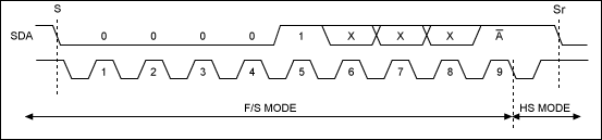
Figure 1. Waveform from fast, standard I²C mode to Hs mode
Built-in I²C Interface Example The PIC18F442 microcontroller (µC) includes an I²C peripheral interface that supports standard and fast I²C modes. Figure 2 shows an application circuit that receives sample data from the ADC (MAX1169) through this interface. After receiving the data, PIC® will send it out through the UART at 115k baud rate, and the data will be collected by the standard serial port of the computer after passing through the RS-232 transceiver (MAX3232E). The file I2C_on_chip_asm.zip contains all the assembly programs that implement the communication of the PIC on-chip I²C interface in fast mode. You can use MPLAB IDE version 6.10.00 to develop the assembly program for the circuit in Figure 2.
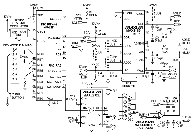
Figure 2. PIC18F442 µC built-in I²C interface to 16-bit ADC (MAX1169)
Bit-by-bit simulation for I²C communication The MAXQ2000 is a low-power 16-bit RISC µC that can implement I²C communication for standard mode, fast mode, and even 1.7MHz Hs mode in bit-by-bit simulation. Figure 3 shows the general schematic of MAXQ2000, which can be used as an I²C host to support three operating modes. To support 1.7MHz Hs mode, the I²C bus in the schematic uses active pull-up. The I2C_bit_bang_asm.zip file contains all the assembly programs needed to emulate the standard, fast mode I²C communication using µC GPIO port.
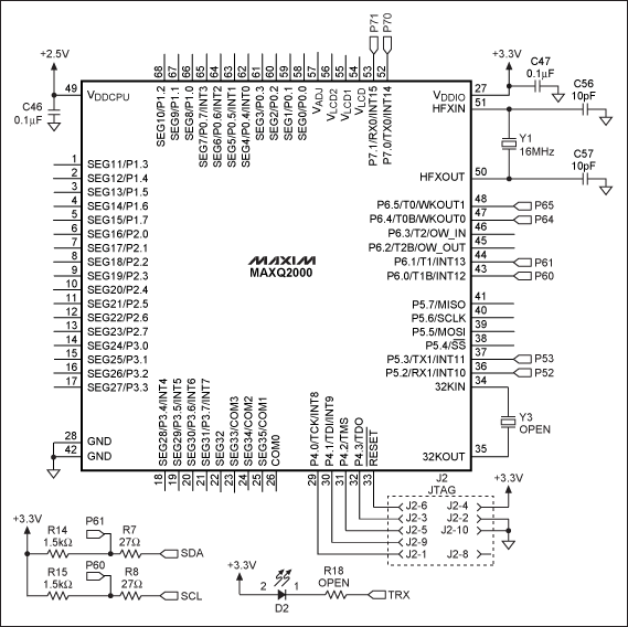
Figure 3. This schematic (based on the MAXQ2000 low-power LCD µC) provides an I²C host capable of operating in standard, fast, or Hs mode
MAXQ2000's I²C firmware has a default clock rate of 100kHz, but the µC's 16MHz system clock can support a bit-by-bit emulated I²C interface operating at 400kHz. The following routine demonstrates the process of capturing interrupt events and handling interrupts in a simple interrupt service routine. The development tool uses MAX-IDE version 1.0 (development date: November 18, 2004), and the software can be downloaded for free from the Maxim website.
The I2C_bit_bang_c.zip file contains the C program source files required by the MAXQ2000 GPIO port bit-by-bit emulation standard, fast mode I²C communication. The routine corresponding to Figure 3 is based on the maxqi2c library file, including maxqi2c.h and maxqi2c.c. After loading the file into the user project, it can support 100kHz or 400kHz I²C communication on any GPIO port. However, when using the C program to generate a specific rate of I²C communication, Y1 in Figure 3 must replace the 15MHz crystal with a 20MHz crystal. This example uses the IAR Embedded Workbench® IDE tool developed for MAXQ2000 version 1.12B (FAE version). Users can download the IAR Embedded Workbench (4K, preliminary version) for MAXQ2000 for free after registering on the IAR website.
The HSI2C_bit_bang_asm_c.zip file contains the assembler and C program required to use the MAXQ2000 GPIO to emulate 1.7MHz Hs mode I²C communication bit by bit. The source code uses a mixture of assembly language and C language code in order to give full play to the advantages of these two programming languages. The assembler helps to optimize the speed, and the C program can make the source code simpler (only a few lines of instructions). The Hs mode has very strict requirements on timing. The I²C receiver function (hsi2cRecv) uses an assembler, and the code is in the hsi2c.asm file.
The main program C code initializes the MAXQ2000 UART with a baud rate of 115.2kbps. In order to achieve 1.7MHz Hs mode I²C communication, Y1 in Figure 3 must use a 20MHz crystal. The main program C code calls the hsi2cRecv function when needed, and uses the printf function to send data through the on-chip UART. The data format is 8-N-1. Rowley CrossWorks IDE version 1.0 (Build 2 Licensed copy) development tool is used here. To obtain CrossWorks IDE tools, please contact Rowley Associates Limited or visit their website.
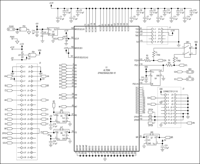
Implementation of I²C IP core peripheral interface DI2CM I²C IP core (developed by Digital Core Design) is widely used in many CPLD and FPGA devices. The DI2CM I²C IP core converts the parallel interface to an I²C interface, and can support the host to work in Hs mode at 3.4MHz. In the application circuit of Fig. 4, Altera® EPM3256AQC208-10 CPLD contains DI2CM IP core. This circuit requires the use of 40MHz crystal (U3) to support 1.7MHz and 3.4MHz Hs mode. The 3-state logic buffer with output enable allows the DI2CM IP core to generate an active pull-up on the SCL line to meet the I²C communication requirements in Hs mode. Logic inversion gate circuits U5, U6, and U7 are used to implement a parallel interface for high-level and low-level memory mapping.
Detailed circuit diagram (PDF, 841KB)
Figure 4. According to the configuration shown in the circuit, the DI2CM IP core in the Altera EPM3256AQC208-10 CPLD can implement the Hs mode I²C host
The HSI2C_IP_core_asm.zip file contains the assembler used to implement Hs mode I²C communication, which is implemented by connecting the 68HC16 memory-mapped parallel interface and the Altera EPM3256 CPLD programmed with the DI2CM IP core. This example uses the Motorola® 68HC macro assembler, version 4.1.
Conclusion Because the I²C bus is the most widely used serial bus in the industry, system designers can get a wealth of proven routines. The implementation schemes are built-in chip, bit-by-bit emulation or IP core, depending on the system processor used. The simplest way to develop using a proven design example is to provide a design reference for the I²C interface in three operating modes.
Appendix 1: Definition of Terms CPLD: Complex Programming Logic Device DI2CM: Hs Mode I²C IP Core FPGA developed by Digital Core Design FPGA: Field Programmable Gate Array GPIO: General Purpose Input / Output hsi2cRecv: Hs Mode I²C receiving function function, using assembler Hs -mode: high-speed I²C mode IC: integrated circuit IDE: integrated development environment IP: intellectual property protection I²C: internal IC bus MAXQ2000: low-power 16-bit RISC microcontroller RS-232: recommended standard # 232 SCL: for I²C bus Hardware serial clock line SDA: hardware serial data line for I²C bus UART: universal asynchronous transceiver µC: microcontroller 8-N-1: 8 bits, no parity, 1 stop bit
We define the delivery quantity that more than 3 square meters as medium size and small volume orders. define the 3-50 square meters orders as small volume orders and the 50-200 square meters orders as medium size orders.
In recent years, there has been increase in demand for low volume so as to obtain first preference for small volume Circuit Board manufacturing; hence we created unique capabilities for catering these services.
We are generally capable of manufacturing from one layer PCB to multilayer as per customer specific board types like FR4, High TG FR-4, Rogers. we are even capable of manufacturing Maximum Panel/Board size 19.7" X 31.5", PCB Thickness 8 mil to 240 mil, Minimum Track Width & spacing 3 mil, Controlled impedance, smallest drill Hole 6 mil, etc.

Medium Size And Small Volume PCB
Medium Size PCB,Small Volume PCB,Economical Medium Size PCB,Medium Size PCB Design
Orilind Limited Company , https://www.orilind.com