Interconnections between the DS21Q41 or DS21Q43 and the Motorola MC68MH360 (QUICC32) are shown in Figure 1. The MC68MH360 can be configured as an HDLC controller implementing protocols such as LAPD for both DS0 channel and the FDL or E1 Sa bits. Any combination of the QUICC32's SCCs and SMCs can be processed through an internal time slot assigner onto one or two Time Division Multiplex channels, TDM A and TDM B. In the configuration shown, TDM channel A is used for timeslots 0-23 (T1) or 0-31 ( E1) and TDM channel B is used for the FDL (T1), or Sa bits (E1). See the MC68MH360 Quad Integrated Communications Controller user's manual for complete details.
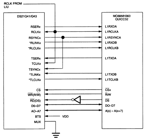
Figure 1. Quad framer-QUICC32 interconnections.
* HDLC on the FDL can be implemented either by TDM CHANNEL B or via the port by the host processor (CPU32 internal to the QUICC32).
DS21Q41, DS21Q43 Notes: Other signals affecting operation of device are not shown. Example circuit has RSYNC in output mode. MC68360 Notes: Other signals affecting operation of device are not shown. Use SI mode register t Set up transmit and receive frame sync delays ( 0-3 clocks) to mask the F-Bit in T1 applications. RFSDA = 1 for DS21Q41, 0 for DS21Q43. Set clock edges for transmit on rising edge and receive on falling edge. CEA = CEB = 0. In the above example, TDM channel A has a common transmit / receive clock and sync. CTRA = 1. Use the TIMESLOT ASSIGNER to ignore Timeslot 0 for the DS21Q43.
- [Compact Design & Family-Sized:]Compact design frees valuable desk space while non-slip grip keeps it from being knocked off. 6 high powered ports lets you charge any combination of phones, tablets or other USB-charged devices simultaneously
Brand Name: OEM
Product Name: Multi USB Charger
Use: Mobile Phone
Place of Origin: Guangdong, China (Mainland)
Port: 6 port
Input: AC100-240V 50/60HZ
Size: 90*70*16mm
Weight: 250g
Materials: PC+ABS
Color: Black/White
Warranty: 1 year
Multi Usb Charger
Multi USB Charger,Multi Usb Wall Charger,Multiple Usb Port Charger,Multi Port USB Charger
Shenzhen Waweis Technology Co., Ltd. , https://www.waweis.com