As the efficiency of power supplies goes up, circuit resistances tend to go down. This can create high-frequency circuits with the potenTIal to generate large voltage overshoots and long decay TImes. It can cause over-voltage stress in the semiconductors, which limits circuit efficiency and reliability.
Snubbing these high-frequency circuits with a simple resistor-capacitor network provides damping, which minimizes ringing and over-voltage stress.
The basic circuit illustrated in Figure 1 serves as a useful model. L1 and C1 form a resonant circuit that is damped by RL. In an actual applicaTIon it is difficult to use the RL for damping, because it is either physically too large or too far away to operate as a real resisTIve load at the ringing frequency, which is usually in the MHz range.
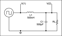
Figure 1.
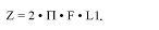
When the circuit in Figure 1 is stimulated with a square wave of 10V peak at V (1), the output at V (2) rings. In this circuit the component stresses are almost doubled. A 10V stimulus results in a 19V response. The plot in Figure 2 shows V (1) (top trace) and V (2) (bottom trace). At this 10MHz ringing frequency it can be difficult to predict how individual circuit components will behave.
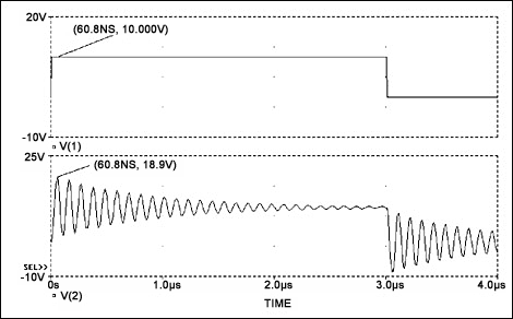
Figure 2.
A very simple method to determine the optimum snubber for a given circuit is to find the components of the LC resonant tank. If the actual tank circuit is not known, try adding a capacitor across suspected nodes until a change of the ringing frequency is observed. If all of the probable nodes have been exhausted in the circuit, try moving a piece of ferrite close to the board. When the highly permeable ferrite interacts with the current loop in the tank, its components can be identified by observing a reduction in frequency. Once the tank capacitor is found, add capacitance across it until the ringing frequency is cut in half. The ringing frequency is cut in halve by squaring the total capacitance value, then adding a series resistance to the capacitor until an acceptable damping is reached. This snubber circuit is formed by RS and CS and shown in Figure 3.
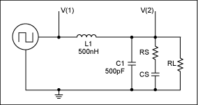
Figure 3.
By knowing how much capacitance is needed to halve the frequency, it is easy to determine the circuit inductance using the formula
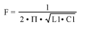 where C1 and F are the circuit's original circuit capacitance and ringing frequency. Because it takes C1 plus 3 added C1's to halve the frequency, the circuit's original capacitance is calculated by dividing the added capacitance by three. The optimum resistor to damp the overshoot is twice the inductive impedance at the new resonant frequency. As an example, if a circuit exhibits a 100ns ring and adding a 1500pf capacitor reduces the period to 200ns, the calculated values ​​for C1 and L2 are 500pF and 500nH, respectively. The inductive impedance is then
 Because the new frequency is 5MHz and L1 is 500nH, it follows that Z equals 15.7Ω. To find the optimum resistor, multiply this inductive impedance by tw for this circuit, 32Ω. The resulting overshoot and decay is greatly reduced, as shown in the plots in Figure 4.
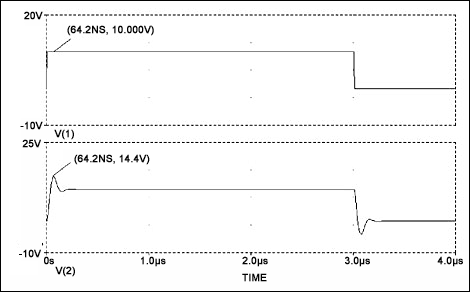
Figure 4.
The power dissipated in the resistor, RS, can be roughly calculated by assuming that the energy stored in the added capacitor is lost in the resistor on each transition, or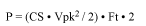 where P is the power dissipated in the resistor in watts, CS is the added capacitance, Vpk is the peak capacitor voltage, and Ft is the switching frequency (two transitions per cycle). In this circuit at 100kHz, RS dissipates approximately 31mW. This is only an approximation to size the resistor and its impact on the circuit. For a more accurate calculation for power dissipation, the true RMS current through the resistor, RS, must be known.
If further reduction in ringing voltage is desired, add capacitance to the tank until a three-fold reduction in ringing frequency is obtained. This reduction will be at the expense of power loss because the circuit needs to drive 9 times more capacitance. For the example above, a value of 4000pF or eight times CS would need to be added to reduce the ringing frequency to 3.33MHz (300nS). The added capacitance divided by eight gives the circuit capacitance, C1, and the inductive impedance is 10.5Ω. Again, to find the RS, the inductive reactance must be multiplied by two. For this circuit 21Ω is the optimum value for RS and it dissipates approximately 63mW. The plot in Figure 5 shows the response of the circuit in Figure 3 with these values.
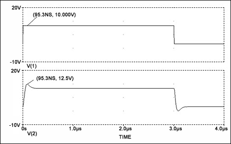
Figure 5.
Although snubbing is lossy it can improve efficiency and reliability. With less ringing, lower voltage parts can be used and the excessive losses due to avalanche effects in semiconductors can be avoided. Circuit noise is also reduced. This method can quickly solve problems in the lab when time for circuit measurement and analysis are not available to the engineer.
Snubbing these high-frequency circuits with a simple resistor-capacitor network provides damping, which minimizes ringing and over-voltage stress.
The basic circuit illustrated in Figure 1 serves as a useful model. L1 and C1 form a resonant circuit that is damped by RL. In an actual applicaTIon it is difficult to use the RL for damping, because it is either physically too large or too far away to operate as a real resisTIve load at the ringing frequency, which is usually in the MHz range.
Figure 1.
When the circuit in Figure 1 is stimulated with a square wave of 10V peak at V (1), the output at V (2) rings. In this circuit the component stresses are almost doubled. A 10V stimulus results in a 19V response. The plot in Figure 2 shows V (1) (top trace) and V (2) (bottom trace). At this 10MHz ringing frequency it can be difficult to predict how individual circuit components will behave.
Figure 2.
A very simple method to determine the optimum snubber for a given circuit is to find the components of the LC resonant tank. If the actual tank circuit is not known, try adding a capacitor across suspected nodes until a change of the ringing frequency is observed. If all of the probable nodes have been exhausted in the circuit, try moving a piece of ferrite close to the board. When the highly permeable ferrite interacts with the current loop in the tank, its components can be identified by observing a reduction in frequency. Once the tank capacitor is found, add capacitance across it until the ringing frequency is cut in half. The ringing frequency is cut in halve by squaring the total capacitance value, then adding a series resistance to the capacitor until an acceptable damping is reached. This snubber circuit is formed by RS and CS and shown in Figure 3.
Figure 3.
By knowing how much capacitance is needed to halve the frequency, it is easy to determine the circuit inductance using the formula
Figure 4.
The power dissipated in the resistor, RS, can be roughly calculated by assuming that the energy stored in the added capacitor is lost in the resistor on each transition, or
If further reduction in ringing voltage is desired, add capacitance to the tank until a three-fold reduction in ringing frequency is obtained. This reduction will be at the expense of power loss because the circuit needs to drive 9 times more capacitance. For the example above, a value of 4000pF or eight times CS would need to be added to reduce the ringing frequency to 3.33MHz (300nS). The added capacitance divided by eight gives the circuit capacitance, C1, and the inductive impedance is 10.5Ω. Again, to find the RS, the inductive reactance must be multiplied by two. For this circuit 21Ω is the optimum value for RS and it dissipates approximately 63mW. The plot in Figure 5 shows the response of the circuit in Figure 3 with these values.
Figure 5.
Although snubbing is lossy it can improve efficiency and reliability. With less ringing, lower voltage parts can be used and the excessive losses due to avalanche effects in semiconductors can be avoided. Circuit noise is also reduced. This method can quickly solve problems in the lab when time for circuit measurement and analysis are not available to the engineer.
The quality is the life of the product. The finest quality are always our pursuit. We special emphasis on the quality of the product. No matter how many quantity or urgent delivery of orders, every order will be good take care of for us. Prompt delivery and competitive price are also our advantages which have earned the trust and respect from our customers. We specialized in the production of LED lights, our products are sold to different countries and regions all over the world.Such as led tube light,g24 led tube light.
G24 Tubes,18W G24 Tubes,13W G24 Tubes,9W Led Tube G24
SHENZHEN KEHEI LIGHTING TECHNOLOGY CO.LTD , https://www.keheiled.com