In this paper, the current LED driver circuit has the limitation of electrolytic capacitor limiting life. A design scheme of high-brightness LED driver circuit with electroless capacitor is proposed. The purpose is to improve the life of the driving power supply, simplify the circuit, reduce the cost and improve the efficiency. Power density.
LED power challenge
As a new type of electric light source, LED has obvious advantages in the production of large-scale luminous three-dimensional characters and illuminating signs, with low control voltage, low cost and high reliability. Although LED products have a growing trend in the domestic and international markets, LED lighting is an emerging industry after all, and it has not been widely popularized. Therefore, LED driving power is inevitably challenging in all aspects: First, due to the positive direction of LED The voltage will change with current and temperature, and its "color point" will drift with current and temperature. In order to ensure the normal operation of the LED, its driver is required to change the input condition and forward voltage. Limit the current. Secondly, if LED dimming is required, pulse width modulation dimming technology is usually used. The typical PWM frequency is 1~3kHz. Finally, the power handling capability of the LED driver circuit must be sufficient, and the function is strong, and can withstand various fault conditions. ,Easy to implement.
The scheme described in this paper adopts the chip of Panasonic Panasonic MIP553 built-in PFC dimmable LED driver circuit, which is combined with external non-isolated bottom edge chopper circuit as the basic circuit structure, and outputs stable current to meet the needs of LED operation. At the same time, a protection circuit is designed to protect the load. The experimental results show that the controller chip can work stably and can achieve a constant voltage output of 27V and a constant current output of 350mA.
The basic working principle of LED power supply
The BUCK converter and IPD control are used to realize the switching power supply, and output constant current and voltage to drive the LED lamp. The overall block diagram of the circuit is shown in Figure 1.
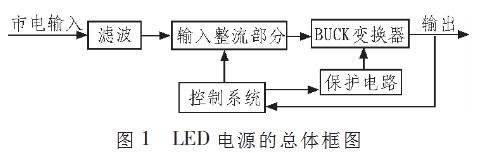
The main circuit part is followed by a filter after the mains supply. Its function is to filter out the higher harmonics in the power supply and the surge in the power supply, so that the control circuit is less interfered by the power supply. The input rectification part adopts an integrated rectifier bridge. The unidirectional conduction characteristic of the diode converts the alternating current whose level is floating up and down at zero to a unidirectional pulsating direct current, and then outputs a direct current voltage under the action of the filter capacitor and the inductor. After the adjustment and control of the MIP553 and BUCK circuits, the voltage for the LEDs is output.
LED power supply specific design
Input circuit design
In order to extend the life of the LED driver and match it to the LED, the electrolytic capacitor in the circuit must be removed.
The design specifications of the circuit are: input AC voltage Vm: 198-264VAC/50Hz; output voltage Vo: 27VDC; output current Io: 0.35A.
The input circuit includes a noise filtering device, a safety device, and an input rectifying device, as shown in FIG.
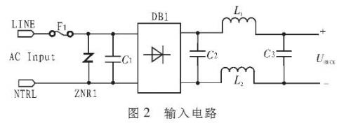
The noise filtering device is mainly composed of a capacitor C1/C2/C3 and an inductor L1, and its function is to reduce electromagnetic interference (EMI) in a frequency band less than 1 MHz. This device can also be linked after AC AC, and the filtering effect is the same before the rectifying device. The safety device consists of a fuse and ZNR1. The fuse mainly prevents the circuit from being cut off to protect the load when the peak current of the circuit is damaged. The ZNR1 is a surge absorber that absorbs static electricity and surge from the input to protect it. The circuit behind. The input rectifier device converts the alternating current into direct current and the input rectifier bridge: the voltage stress of the rectifier bridge diode is:
Consider the margin, choose TSC GBL205 (VR=600V, IFAN=1A).
Output circuit design
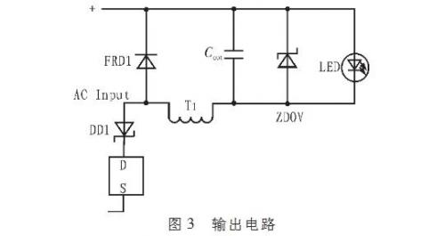
The output circuit consists of a basic BUCK circuit and a Zener diode DD1. As shown in Figure 3.
BUCK converter and its advantages
Buck converter, also known as buck converter, series switching regulator, three-terminal switching buck regulator, is a single-tube non-isolated DC/DC converter with output voltage equal to or less than the input voltage.
The input current is in operation, when the switch is closed, is>0; when the switch is open, is=0, so is is pulsating, but the output current io is continuous and smooth under the action of inductor, diode and capacitor. of. Particularly suitable for providing operating current for LEDs.
FRD1 selection criteria: The rated current is greater than 2 times the output current, the rated voltage is greater than the input voltage, and the reverse recovery time is also within 100 ns. Consider the margin, the parameters of FRD1 are: 15A, 600V, trr=50ns. The method selects T1 and Cout, then the parameters are: T1: 680μH; Cout: 1μF, 50V.
Zener diode DD1
In the range of low input voltage, if there is no such reverse device like DD1, then there will be reverse current flowing through the IPD when the switch is turned off, and IPD is not allowed to have such current, because this A reverse current will cause damage to the IPD.
Each stress received by DD1: IDD>2·Io=2×0.35=0.7A, UDD>Uo, reverse recovery time trr<100ns. Considering the margin, the selected parameter is: 3A/60V/75ns.
protect the circuit
MIP553 has built-in protection circuit for overvoltage, overcurrent, overheat, and LED short circuit, but there is no protection circuit design when the LED is open. The idea of ​​the protection circuit when the LED is open is mainly the Zener diode protection, the triode protection, the bias coil protection, etc. Considering the cost and structure, the protection circuit with the Zener diode is selected in the paper. Its circuit diagram is shown in Figure 3. When the LED is open, the output voltage rises. If the output circuit has a Zener diode protection circuit, the Zener diode clamps the LED voltage below the diode's voltage drop, which prevents the output capacitor from being destroyed.
Control circuit design
The control circuit consists of MIP553 and its peripheral circuits, as shown in Figure 4.
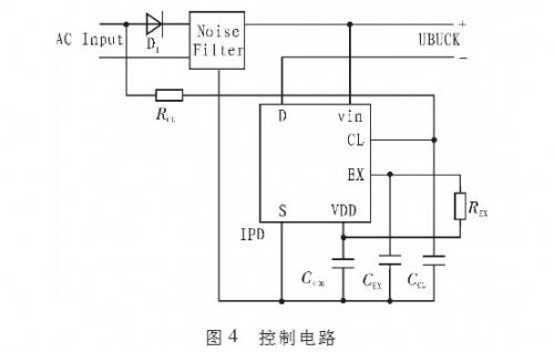
MIP553 chip realizes wide voltage 85~277V/AC input, built-in MOS, simple and stable structure, can eliminate electrolytic capacitor, support isolated or non-isolated scheme, single power output power 6~30W, constant current output <1A. Power supply has overvoltage Overcurrent, overheat protection, high safety and stability, small size, low heat, power efficiency ≥80%, power factor ≥95%, THD<20%.
The drain current of the MIP553 is controlled by pins CL and EX, so the setting of the resistors RCL and REX connecting these two pins will directly affect the drain current. The maximum drain current can be determined by REX. Considering that this maximum drain current flows through the LED, care should be taken when setting the reference value.
REX=(VDD(ON)-VEXH)/IEX=(6.5-2.8)/103=36kΩ (3)
Among them, assume input voltage 100V, output voltage 28V, current: 400mA, maximum drain current is set to 1.0A.
The functions of CVDD, CEX, and CCL are to stabilize the operation of the MIP 553 and suppress external noise. Therefore, its value should be chosen properly. CVDD, stable VDD voltage, suppress LED flicker, characteristics are not affected by temperature, no additional noise, reference standard value is between 1~10μF; CEX, suppress external noise into EX pin, its reference standard value is 470 ~1000pF; CCL, suppress external noise into the CL pin, if its value is too large, then the pF value will be seriously affected, so its value should be less than 1000pF.
Simulation results
The circuit is simulated by Multisim, and the result is shown in Figure 5.

As can be seen from Figure 5, the output voltage is stable at 27V and the current is stable at 0-35A, which meets the design requirements.
This paper introduces the LED driver power supply designed by MIP553, and proves the stability of its output current through simulation, which has a good application prospect.
1. An open structure of heating elements with half round stainless steel
reflectors for an optimal use of energy.
2. The Gyros will change direction automatice, if there is a force.
3. Removable and detachable parts for easy clean.
4. The particular broiling result is obtained by alternating heating and
cooling down. The meat fibres do not harden, and the gravy is flavoured
by the spices. This cooking mode results in very healthy meat.
5. The Vertical Grill allows broiling meat layers, shashlik, party sausages,
poultry and fish with few attachments.
6. The Skewers and Gyros go in opposite direction so that the food could
be heated more well.
7. Power: 1400W

Smokeless Electric Grill,Electric Multi Grill,Non-Stick Electric Grill,Electric Bbq Grill
Housoen Electric Manufacture Co., Ltd. , https://www.housoenappliances.com